Supercharge Your Innovation With Domain-Expert AI Agents!

VDMOS device and preparation method thereof

A device and type of technology, applied in the field of VDMOS, which can solve problems such as reduced breakdown capability and increased current

Pending Publication Date: 2020-12-11
SIEN QINGDAO INTEGRATED CIRCUITS CO LTD
View PDF3 Cites 0 Cited by
  • Summary
  • Abstract
  • Description
  • Claims
  • Application Information

AI Technical Summary

Problems solved by technology

The root cause of UIS failure is that the opening of the parasitic NPN causes an increase in current and a decrease in breakdown capability.
Therefore, to suppress the failure of the super-junction UIS is to suppress the turn-on of the parasitic NPN transistor, and try to ensure that the product of the current and the resistance flowing through the P base region (body-doped region) when the device is turned off is less than the turn-on voltage of the PN junction. At present, the usual practice is to increase the N+ region The doping concentration of the lower volume doped region, but the concentration of the P base region will increase the VDMOS threshold voltage

Method used


Image

  • VDMOS device and preparation method thereof
  • VDMOS device and preparation method thereof

Examples


Embodiment Construction

[0030] In order to make the purpose, technical solutions and advantages of the embodiments of the present invention clearer, the technical solutions in the embodiments of the present invention will be clearly and completely described below in conjunction with the drawings in the embodiments of the present invention. Obviously, the described embodiments It is a part of embodiments of the present invention, but not all embodiments. Based on the embodiments of the present invention, all other embodiments obtained by those skilled in the art without creative efforts fall within the protection scope of the present invention.

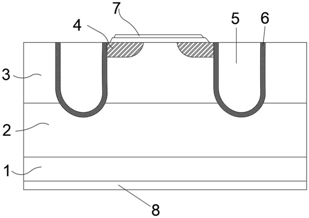
[0031] An embodiment of the present invention provides a VDMOS device that improves the UIS capability of the VDMOS device, and the VDMOS device includes a first-type doped substrate, a drift region, a body doped region, a source region, and a gate oxide layer; the drift region The source region is doped with the first type, the doping concentration of the so...


PUM

PropertyMeasurementUnit
thicknessaaaaaaaaaa

Abstract

The invention provides a VDMOS device and a preparation method thereof. The VDMOS device comprises a substrate with first type doping, a drift region, a body doping region, a source region and a gateoxide layer, wherein the drift region and the source region are doped in a first type, and the doping concentration of the source region is greater than that of the drift region; the body doped regionis doped in a second type, the doping concentration of the body doped region is greater than 5 * 10<18>cm <3>, and the dielectric constant of the gate oxide layer is greater than 25; according to theinvention, the P-type doping concentration of the body doped region is improved, the regional resistance of the body doped region is reduced, the threshold voltage is not obviously increased, and thethickness of the gate oxide layer does not need to be increased or decreased, so the opening of the BJT is inhibited to further improve the UIS capability.

Description

technical field [0001] The invention relates to the technical field of VDMOS, in particular to a structure and a method for changing the UIS capability of a VDMOS device. Background technique [0002] Vertical double diffused metal oxide semiconductor field effect transistors (VDMOS) include planar type VDMOS and trench type VDMOS. Trench VDMOS is a power device with a wide range of uses. Its drain and source poles are arranged on both sides of the device, and the current flows vertically inside the device, thereby increasing the current density and improving the rated current. The on-resistance per unit area is relatively low. Small. Conventional trench-type VDMOS manufacturing methods generally include forming a gate trench inside the epitaxial layer of a silicon substrate, forming a gate oxide layer and polysilicon inside the gate trench, and then performing ion implantation to form a gate trench inside the epitaxial layer. Then implant different types of ions to form s...

Claims


Application Information

Patent Timeline
Patent Type & Authority Applications(China)
IPC IPC(8): H01L29/06H01L29/78H01L21/336
CPCH01L29/7813H01L29/0684H01L29/66068H01L29/66734
Inventor 迟延庆
Owner SIEN QINGDAO INTEGRATED CIRCUITS CO LTD
Features
  • R&D
  • Intellectual Property
  • Life Sciences
  • Materials
  • Tech Scout
  • Unparalleled Data Quality
  • Higher Quality Content
  • 60% Fewer Hallucinations
Learn More