

Infrared detector and preparation method thereof
A technology of infrared detectors and nanopillars, which is applied in the direction of semiconductor devices, final product manufacturing, sustainable manufacturing/processing, etc., can solve the problems of low efficiency of infrared detectors and difficulty in meeting the needs of deep infrared detection, and achieve bias electric field Uniform distribution, improved absorption efficiency, and improved extraction efficiency
- Summary
- Abstract
- Description
- Claims
- Application Information
AI Technical Summary
Problems solved by technology
Method used
Image



Examples
preparation example Construction
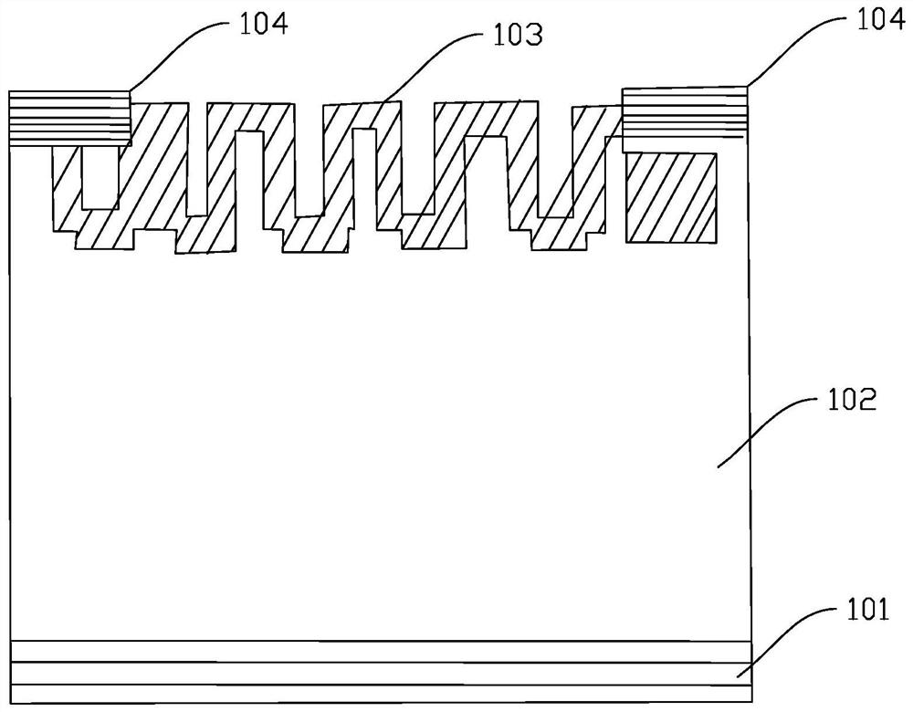
[0030] In some specific embodiments of the present invention, the infrared detector and the preparation method thereof of the above-mentioned embodiments of the first aspect of the present invention are used. Include steps:
[0031] S201: Spin-coat photoresist, uniformly spin-coat a layer of photoresist on the infrared light incident surface on the Si-based infrared detector 102 with a spin coater;
[0032] S202: exposure, using a photolithography machine for exposure and development;
[0033] S203: Wet etching, using an etching solution to etch to obtain an array of Si nanopillars;
[0034] S204: cleaning, removing the photoresist, and cleaning the etching solution;
[0035] S205: Ge film preparation, using a coating machine to evaporate a Ge film on the Si nano-column array;
[0036] S206: Step annealing, including crystallization and infiltration;
[0037] S207: Evaporating electrodes: Evaporating electrodes on the back and front surfaces respectively, and performing al...
PUM
| Property | Measurement | Unit |
|---|---|---|
| Diameter | aaaaa | aaaaa |
| Height | aaaaa | aaaaa |
| Thickness | aaaaa | aaaaa |
Abstract
Description
Claims
Application Information