Dielectric waveguide filter and manufacturing method thereof

A dielectric waveguide and filter technology, which is applied in the field of dielectric waveguide filters and their production, can solve the problems of limited coupling adjustment methods, small coupling adjustment range, and susceptibility to interference, so as to improve anti-interference ability and reduce follow-up Processing, high precision effect

Active Publication Date: 2020-12-11
CHAOZHOU THREE CIRCLE GRP
View PDF9 Cites 1 Cited by
  • Summary
  • Abstract
  • Description
  • Claims
  • Application Information

AI Technical Summary

Problems solved by technology

[0005] In order to solve the above problems, the purpose of the present invention is to provide a dielectric waveguide filter to solve the problem that the adjustment method of the coupling amount of the negative coupling structure is limited, the adjustment range of the coupling amount is small, and it is easily affected by the second harmonic in the low frequency band. The influence of interference, the problem of poor performance of the whole filter

Method used


Image

  • Dielectric waveguide filter and manufacturing method thereof
  • Dielectric waveguide filter and manufacturing method thereof
  • Dielectric waveguide filter and manufacturing method thereof

Examples


Embodiment Construction

[0042] The specific implementation manners of the present invention will be further described in detail below in conjunction with the accompanying drawings and embodiments. The following examples are used to illustrate the present invention, but are not intended to limit the scope of the present invention.

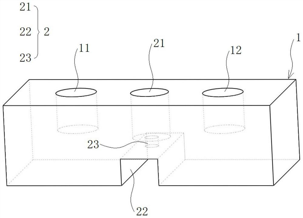
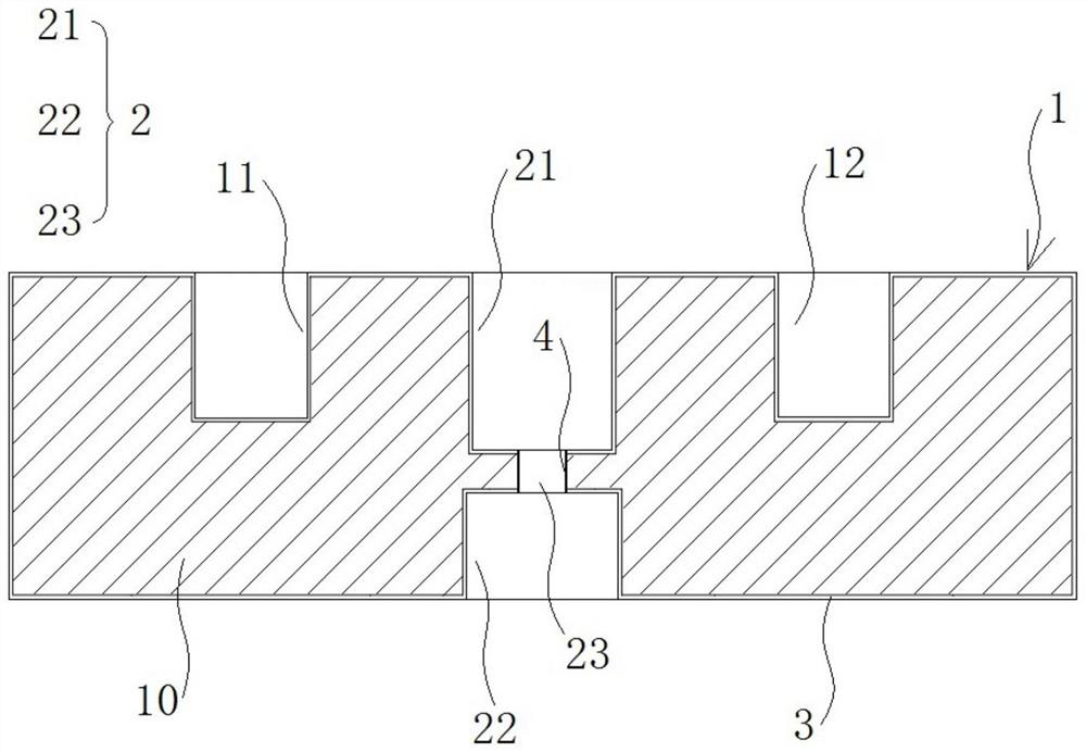
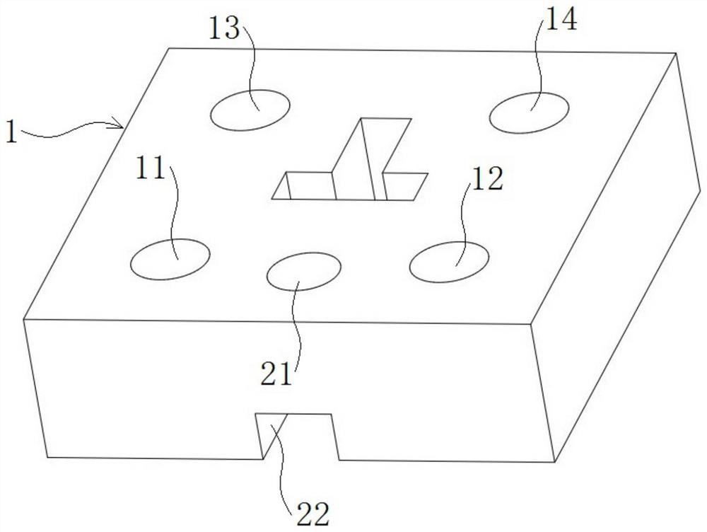
[0043] Specific embodiment 1 of the dielectric waveguide filter of the present invention, as Figure 1 to Figure 4As shown, in this embodiment, the dielectric waveguide filter 1 is composed of a resonant structure part and a negative coupling structure part, wherein, figure 1 , figure 2 shows a local configuration involving two FM blind vias and a negative coupling structure, image 3 , Figure 4 Then it shows the complete configuration of the dielectric waveguide filter 1 composed of four FM blind holes and the negative coupling structure. The dielectric waveguide filter 1 includes a dielectric body 10, a first FM blind hole 11 and a second FM blind hole 12 arranged ...


PUM

PropertyMeasurementUnit
Thicknessaaaaaaaaaa
Axial dimensionaaaaaaaaaa

Abstract

The invention provides a dielectric waveguide filter and a manufacturing method thereof, and relates to the field of filters. The dielectric waveguide filter comprises a dielectric body, a first frequency modulation blind hole, a second frequency modulation blind hole and a negative coupling structure, the first frequency modulation blind hole and the second frequency modulation blind hole are formed in the dielectric body, the negative coupling structure is arranged on the dielectric body and located between the first frequency modulation blind hole and the second frequency modulation blind hole, and a conducting layer is arranged on the surface of the dielectric body; the negative coupling structure comprises a negative coupling blind hole, a negative coupling blind groove and a communicating hole, the axial direction of the negative coupling blind hole is parallel to the axial directions of the first frequency modulation blind hole and the second frequency modulation blind hole, thenegative coupling blind groove is formed in the opposite side, back to the negative coupling blind hole, of the dielectric body, and the communicating hole is connected between the negative couplinghole and the negative coupling blind groove; and an insulating ring region is arranged on the inner wall of the communicating hole. When the boundary dimension of the communicating hole changes, the shapes and dimensions of a signal propagation channel and the insulating ring region change at the same time, so that the coupling amount can be adjusted in a larger range, and the performance of the whole filter is better.

Description

technical field [0001] The invention relates to the technical field of filters, in particular to a dielectric waveguide filter and a manufacturing method thereof. Background technique [0002] In the communication industry, the base station is a key device in the entire mobile communication system, and its products are updated and iterated rapidly. Among them, the filter in the base station is a component used to select specific frequency radio waves and suppress other frequency radio waves. [0003] Traditional metal cavity filters cannot meet the requirements of miniaturization, low cost, high integration and high Q value, especially, they cannot meet the more stringent suppression requirements of 5G technology. Subsequently, a new type of filter with a transmission zero point was developed. For example, the Chinese utility model patent with the authorized announcement number CN210468049U and the authorized announcement date of 2020.05.05 discloses a capacitive coupling s...

Claims


Application Information

Patent Timeline
IPC IPC(8): H01P1/212H01P11/00
CPCH01P1/212H01P11/007
Inventor 李钢
Owner CHAOZHOU THREE CIRCLE GRP
Why Eureka
Try Eureka