Bypass diode for solar junction box

A bypass diode and junction box technology, applied in the field of diodes, can solve the problems of high-temperature battery failure, limited packaging, small cross-sectional area, etc., and achieve the effects of expanding heat dissipation area, long service life and convenient use

Pending Publication Date: 2020-12-18
山东元捷电子科技有限公司
View PDF0 Cites 1 Cited by
  • Summary
  • Abstract
  • Description
  • Claims
  • Application Information

AI Technical Summary

Problems solved by technology

[0005] Aiming at the problems existing in the prior art, the object of the present invention is to provide a bypass diode for a solar junction box. By assembling the chip parallel to the wire, a semiconductor chip of a larger size can be placed in the same external dimension, improving The rated power of the product, and increasing the copper wire area inside the product, expanding the heat dissipation area of ​​the chip, can effectively reduce the product failure rate, and solve the problem that the diameter of the cylindrical package limits the packaging of large-size chips, which cannot be realized Encapsulation of chips with larger power size. At the same time, because the cross-sectional area of ​​the copper wire is too small, it is not conducive to the heat dissipation of the chip, and it is easy to cause the failure of high-temperature batteries.

Method used


Image

  • Bypass diode for solar junction box
  • Bypass diode for solar junction box
  • Bypass diode for solar junction box

Examples


Embodiment Construction

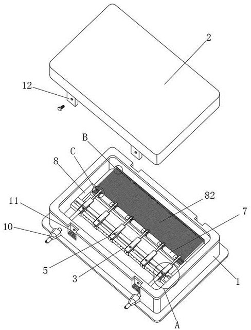
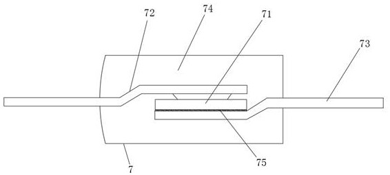
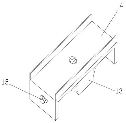
[0037] The following will clearly and completely describe the technical solutions in the embodiments of the present invention in conjunction with the accompanying drawings in the embodiments of the present invention; obviously, the described embodiments are only part of the embodiments of the present invention, not all embodiments, based on The embodiments of the present invention and all other embodiments obtained by persons of ordinary skill in the art without making creative efforts belong to the protection scope of the present invention.

[0038] In the description of the present invention, it should be noted that the orientations or positional relationships indicated by the terms "upper", "lower", "inner", "outer" and "top / bottom" are based on the orientations or positional relationships shown in the drawings. The positional relationship is only for the convenience of describing the present invention and simplifying the description, but does not indicate or imply that the ...


PUM


Abstract

The invention discloses a bypass diode for a solar junction box, and belongs to the field of diodes. The diode comprises a box body, a box cover is fixedly connected to the top of the box body, a sliding rail is fixedly connected to the bottom of the inner wall of the box body, and six connecting seats are movably connected to the surface of the sliding rail. Connecting reeds are fixedly connectedto the tops of the six connecting seats, connecting pins are fixedly connected to the tops of the connecting reeds, a diode body is fixedly connected between every two adjacent connecting pins, two connectors are fixedly connected to one side of the box body, and leads are fixedly connected to one sides of the two connectors. According to the invention, chips are assembled in parallel with the leads, and semiconductor chips with larger sizes can be placed in the same boundary dimension so that rated power of a product is improved, an area of copper leads in the product is increased, a heat dissipation area of the chips is enlarged, and a failure rate of the product can be effectively reduced.

Description

technical field [0001] The invention relates to the field of diodes, in particular to a bypass diode for a solar junction box. Background technique [0002] A photovoltaic power generation device usually consists of several photovoltaic modules. Photovoltaic modules are composed of photovoltaic power generation unit groups in series according to the required voltage, and photovoltaic power generation unit groups are composed of photovoltaic power generation units in series. When photovoltaic modules receive solar energy, when some photovoltaic power generation units cannot receive solar energy or are damaged In this case, a high power consumption state ("hot spot") will appear, which will damage the photovoltaic power generation unit and cause power generation failure. Therefore, photovoltaic modules need to use photovoltaic bypass diode circuits to protect photovoltaic modules and maintain the normal operation of photovoltaic power generation devices , the photovoltaic byp...

Claims


Application Information

Patent Timeline
Patent Type & Authority Applications(China)
IPC IPC(8): H02S40/34H01L29/861H01L23/367H01L23/48
CPCH01L23/3672H01L23/3677H01L23/48H01L29/861H02S40/34H02S40/345Y02E10/50
Inventor 任志红
Owner 山东元捷电子科技有限公司
Why Eureka
Try Eureka