A semiconductor process equipment

A process equipment and semiconductor technology, applied in the direction of crystal growth, chemical reactive gas, single crystal growth, etc., can solve the problem of high deposition speed of epitaxial layer at the edge of the substrate, and achieve the effect of improving uniformity

Active Publication Date: 2022-07-22
BEIJING NAURA MICROELECTRONICS EQUIP CO LTD
View PDF0 Cites 0 Cited by
  • Summary
  • Abstract
  • Description
  • Claims
  • Application Information

AI Technical Summary

Problems solved by technology

However, this solution will also result in the deposition rate of the epitaxial layer at the edge of the substrate being greater than the thickness of the epitaxial layer deposited in the central area

Method used


Image

  • A semiconductor process equipment
  • A semiconductor process equipment
  • A semiconductor process equipment

Examples


Embodiment Construction

[0023] The specific embodiments of the present invention will be described in detail below with reference to the accompanying drawings. It should be understood that the specific embodiments described herein are only used to illustrate and explain the present invention, but not to limit the present invention.

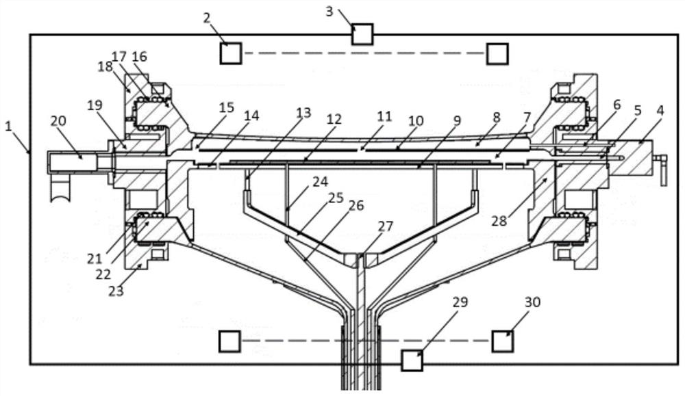
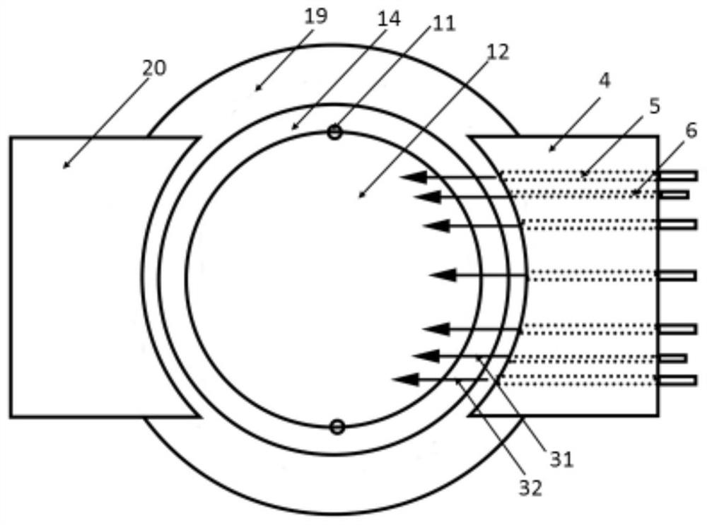
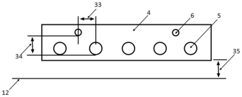
[0024] To solve the above problems, such as figure 1 As shown, the present invention provides a semiconductor process equipment, including a process chamber, a carrier plate 9 and a process spacer 10 arranged in the process chamber, the process spacer 10 and the carrier plate 9 are arranged in parallel, and the process spacer 10 and the carrier plate 10 are arranged in parallel. A main airflow area 7 is formed between the trays 9 , and a secondary airflow area 8 is formed on the side of the process partition 10 away from the carrier tray 9 (between the process partition 10 and the upper cover 16 ).

[0025] The inner wall of the process chamber has an exhaust port and a...


PUM


Abstract

The invention provides a semiconductor process equipment, comprising a process chamber and a carrier plate arranged in the process chamber, an exhaust port and a plurality of air inlets are provided on the inner wall of the process chamber, and the plurality of air inlets include at least one main The air inlet and at least one auxiliary air inlet, the semiconductor process equipment also includes a process partition, the process partition is arranged in parallel with the carrier plate, a main airflow area is formed between the process partition and the carrier plate, and the process partition is away from the carrier plate. A secondary air flow area is formed on one side, the main air inlet is matched with the main air flow area, the secondary air inlet is matched with the secondary air flow area, and at least one air guide hole is formed on the process partition which penetrates the process partition along the thickness direction. The semiconductor process equipment provided by the invention can accurately change the deposition speed of the epitaxial layer at the partial position of the substrate through the air guide holes while avoiding the mutual impact of the first process gas and the second process gas, thereby improving the uniformity of the deposition of the epitaxial layer on the substrate. and controllability of the deposition rate of the epitaxial layer at each position of the substrate.

Description

technical field [0001] The present invention relates to the field of semiconductor process equipment, in particular, to a semiconductor process equipment. Background technique [0002] Vapour phase epitaxy is a common epitaxial growth technology, which can grow on a single crystal substrate with a different conductivity type, resistivity and structure from the substrate substrate, and the thickness and resistivity are different. Controllable, single crystal layer that can meet a variety of different requirements, can greatly improve the flexibility and performance of device design, and has a wide range of semiconductor functional devices (such as IGBT, CMOS, digital storage DRAM, microprocessors, etc.) application prospects. [0003] In the vapor phase epitaxy growth process, the stability and uniformity of the epitaxial layer thickness is closely related to the gas flow field in the process chamber. In order to improve the uniformity of the thickness of the epitaxial laye...

Claims


Application Information

Patent Timeline
Patent Type & Authority Patents(China)
IPC IPC(8): C30B25/08C30B25/14C30B25/12C30B25/16
CPCC30B25/08C30B25/14C30B25/165C30B25/12
Inventor 徐柯柯
Owner BEIJING NAURA MICROELECTRONICS EQUIP CO LTD
Why Eureka
Try Eureka