Sb compound-based medium-short wave double-color infrared detector and preparation method thereof

An infrared detector, short-wave infrared technology, applied in the direction of semiconductor devices, final product manufacturing, sustainable manufacturing/processing, etc., can solve the problems of increasing the complexity of component adjustment, limited improvement effect, and reduced repeatability, etc., to achieve improved Anti-interference and detection effect, simple structure, strong repeatability effect

Pending Publication Date: 2021-01-01
YUNNAN NORMAL UNIV
View PDF0 Cites 6 Cited by
  • Summary
  • Abstract
  • Description
  • Claims
  • Application Information

AI Technical Summary

Problems solved by technology

[0005] The M-type InAs / GaSb / AlSb / GaSb superlattice in the PMP structure infrared detector can reduce the dark current and improve the quantum efficiency theoretically, but the improvement effect is limited, and the introduction of the AlSb component increases the complexity of its composition adjustment and is The reproducibility is reduced, and its cost is increased. In summary, the medium-wave infrared InAs / GaSb superlattice and the short-wave infrared GaSb material are combined to prepare a repeatable, low-cost, high-performance medium-short wave two-color Infrared detectors are necessary

Method used


Image

  • Sb compound-based medium-short wave double-color infrared detector and preparation method thereof
  • Sb compound-based medium-short wave double-color infrared detector and preparation method thereof
  • Sb compound-based medium-short wave double-color infrared detector and preparation method thereof

Examples


Embodiment

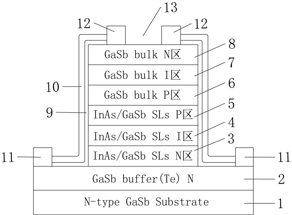
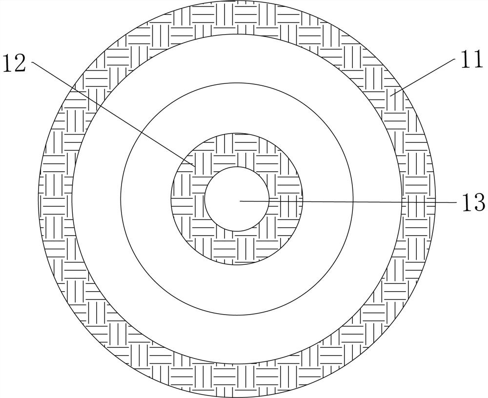
[0044] Such as figure 1 , figure 2 As shown, a Sb compound-based medium-short-wave dual-color infrared detector structure from top to bottom is GaSb substrate-1, Te-doped N-type GaSb buffer layer-2, mid-wave infrared InAs / GaSb superlattice N-type Layer-3, mid-wave infrared InAs / GaSb superlattice unintentionally doped absorbing layer-4, mid-wave infrared InAs / GaSb superlattice P-type layer-5, short-wave infrared GaSb bulk material P-type layer-6, short-wave infrared Unintentionally doped absorbing layer of GaSb bulk material—7, N-type layer of short-wave infrared GaSb bulk material—8, sulfide layer—9 and SiO2 passivation layer—10 on the side wall of the step, upper mesa of the step and lower mesa of the step, and The mesa is provided with a metal upper electrode-12 and a light hole-13, wherein the metal upper electrode-12 is in contact with the short-wave infrared GaSb bulk material N-type layer-8, and the lower mesa of the steps is provided with a metal lower electrode-11 an...


PUM

PropertyMeasurementUnit
depthaaaaaaaaaa
thicknessaaaaaaaaaa

Abstract

The invention discloses an Sb compound-based medium-short wave double-color infrared detector and a preparation method thereof, the structure of the Sb compound-based medium-short wave double-color infrared detector provided by the invention comprises a GaSb substrate and an epitaxial structure deposited on the GaSb substrate, the epitaxial structure comprises a Te doped N-type GaSb buffer layer,a medium-wave infrared InAs / GaSb superlattice N-type layer, a medium-wave infrared InAs / GaSb superlattice unintentionally doped absorption layer, a medium-wave infrared InAs / GaSb superlattice P-type layer, a short-wave infrared GaSb body material P-type layer, a short-wave infrared GaSb body material unintentionally doped absorption layer and a short-wave infrared GaSb body material N-type layer.According to the invention, an NIPPIN type back-to-back double-diode structure is adopted, so that short-wave infrared and medium-wave infrared can be respectively detected through bias modulation. The absorption coefficient can be improved by adopting the two absorption layers with the thickness larger than or equal to 1.5 microns, so that the quantum efficiency and the detection rate are improved, and the detector is simple in structure, simple in preparation process, high in repeatability, low in cost and beneficial to large-scale production.

Description

technical field [0001] The invention belongs to the field of infrared photoelectric materials and devices, and in particular relates to a Sb compound-based medium-short-wave two-color infrared detector and a preparation method thereof. Background technique [0002] Infrared detection is a passive detection technology, which has extremely important applications in military and civilian fields. Among them, the dual-color infrared detection can obtain information of different bands of the target, improve anti-jamming performance and recognition ability, and reduce false alarm rate. Under normal circumstances, the wavelengths of most objects' own radiation are in the range of short-wave infrared (1-3μm) and medium-wave infrared (3-5μm), so short- and medium-short dual-color infrared detectors are widely used in infrared early warning, missile guidance, medical imaging and other fields. There are a wide range of applications. [0003] At present, the materials used for mid-wave...

Claims


Application Information

Patent Timeline
Patent Type & Authority Applications(China)
IPC IPC(8): H01L31/105H01L31/032H01L31/0352H01L31/18
CPCH01L31/0324H01L31/035236H01L31/035272H01L31/105H01L31/18Y02P70/50
Inventor 马晓乐郭杰郝瑞亭艾尔肯·阿不都瓦衣提魏国帅孙帅辉方水柳李晓明王云鹏刘慧敏王国伟徐应强牛智川
Owner YUNNAN NORMAL UNIV
Why Eureka
Try Eureka