Chip layout structure of half-bridge IGBT module

A chip layout and chip technology, applied in semiconductor devices, semiconductor/solid-state device components, electrical components, etc., can solve problems such as large difference in the peak value of turn-on current, reducing the rate of difference in peak value of turn-on current between chips, and easy bonding process. , to reduce the impact, facilitate long-term stable operation, and improve the current sharing performance.

Active Publication Date: 2021-01-05
NARI TECH CO LTD
View PDF2 Cites 1 Cited by
  • Summary
  • Abstract
  • Description
  • Claims
  • Application Information

AI Technical Summary

Problems solved by technology

[0005] The purpose of the present invention is to provide a chip layout structure of a half-bridge IGBT module, which can effectively reduce the and the bonding process is easy to process

Method used


Image

  • Chip layout structure of half-bridge IGBT module
  • Chip layout structure of half-bridge IGBT module
  • Chip layout structure of half-bridge IGBT module

Examples


Embodiment Construction

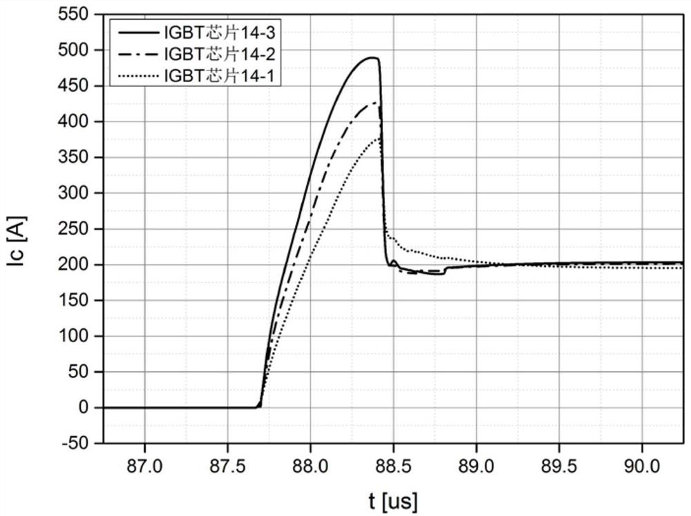
[0024] The present invention provides a new chip layout structure of the half-bridge IGBT module, by changing the position of the gate of the IGBT chip and the position of the gate bonding wire on the gate signal copper layer, so as to reduce the peak value of the turn-on current between the chips purpose of differential rate.

[0025] Concrete structure of the present invention is:

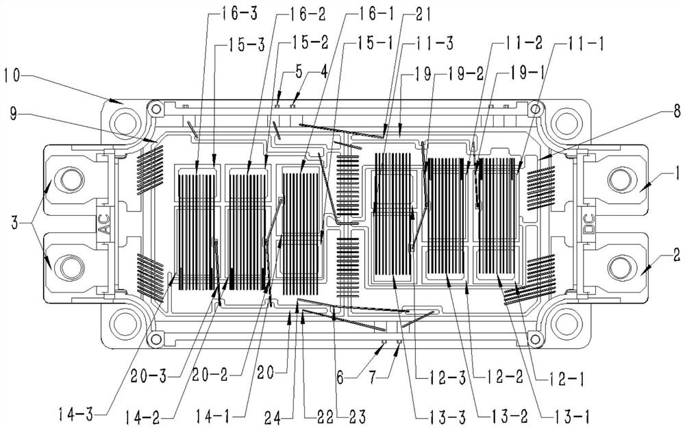
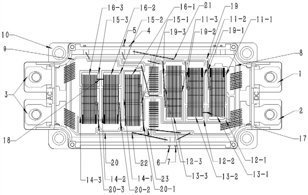
[0026]A chip layout structure of a half-bridge IGBT module, including a positive terminal, a negative terminal, and an output terminal connected to an external circuit when in use; an upper bridge signal terminal and its return line terminal, and a lower bridge signal terminal connected to a drive control circuit when in use and its return terminals. The upper and lower half bridges of the IGBT module are composed of three sets of IGBT chips and FRD chips connected in antiparallel to them. The upper bridge IGBT chip and the FRD chip are connected on the front side of the chip through the bondin...


PUM


Abstract

The invention discloses a chip layout structure of a half-bridge IGBT module. The structure comprises an upper bridge IGBT chip and a lower bridge IGBT chip, the upper bridge IGBT chip and the lower bridge IGBT chip are connected with an FRD chip through bonding wire groups to realize chip front connection, grids are positioned on the left side of the IGBT chip, and the reverse sides of the upperbridge IGBT chip and the lower bridge IGBT chip are welded on an upper bridge DCB substrate; dgrids of the lower bridge IGBT chip are all located on the right sides of the IGBT chip, and the upper andlower IGBT chips and the FRD chip are distributed in a central symmetry mode relative to the module. The drop points of the bonding wires of an upper half-bridge signal terminal and a lower half-bridge signal terminal are located on the grid signal copper layers of the upper half-bridge and the lower half-bridge respectively, and the drop points of the bonding wires of the upper half-bridge and the lower half-bridge are located between the drop points of the grid bonding wires of the two non-adjacent IGBT chips on the grid signal copper layers. Simulation shows that the peak current difference rate of the three IGBT chips is reduced from 30% to 9.3%, so that the current sharing performance of the chips is improved; the reduction of the maximum peak current of the chips reduces the impactof the turn-on current on the chips, and facilitates the long-term stable operation of the chips.

Description

technical field [0001] The invention belongs to the technical field of controllable power semiconductor devices, and in particular relates to a chip layout structure of a half-bridge IGBT module. Background technique [0002] The half-bridge IGBT module is a modular semiconductor product composed of IGBT (insulated gate bipolar transistor chip) and FRD (fast recovery diode chip) bridged and packaged through a specific half-bridge circuit. The current of the IGBT device can be increased by connecting multiple chips in parallel. grade. The parallel current sharing effect of the internal chips of the IGBT device will have a great impact on the performance of the device. The current imbalance of each chip will generate more power consumption. In severe cases, the IGBT device will fail or even be damaged, reducing the stability of the device and system operation. . [0003] The chip layout structure of the traditional half-bridge IGBT module is as follows: figure 1 As shown, t...

Claims


Application Information

Patent Timeline
Patent Type & Authority Applications(China)
IPC IPC(8): H01L25/18H01L23/49
CPCH01L25/18H01L23/49H01L2924/19107H01L2224/49111H01L2224/48139
Inventor 潘政薇李宇柱姚二现董长城骆健
Owner NARI TECH CO LTD
Why Eureka
Try Eureka