Thin film semiconductor device

A thin-film semiconductor and thin-film transistor technology, applied in semiconductor devices, electrical solid-state devices, transistors, etc., can solve problems such as weakening the advantages of low-cost glass substrates

Inactive Publication Date: 2003-09-24
JAPAN DISPLAY INC
View PDF5 Cites 0 Cited by
  • Summary
  • Abstract
  • Description
  • Claims
  • Application Information

AI Technical Summary

Problems solved by technology

However, this approach is not always practical because it greatly reduces the advantage of using low-cost glass substrates

Method used


Image

  • Thin film semiconductor device
  • Thin film semiconductor device
  • Thin film semiconductor device

Examples


Embodiment Construction

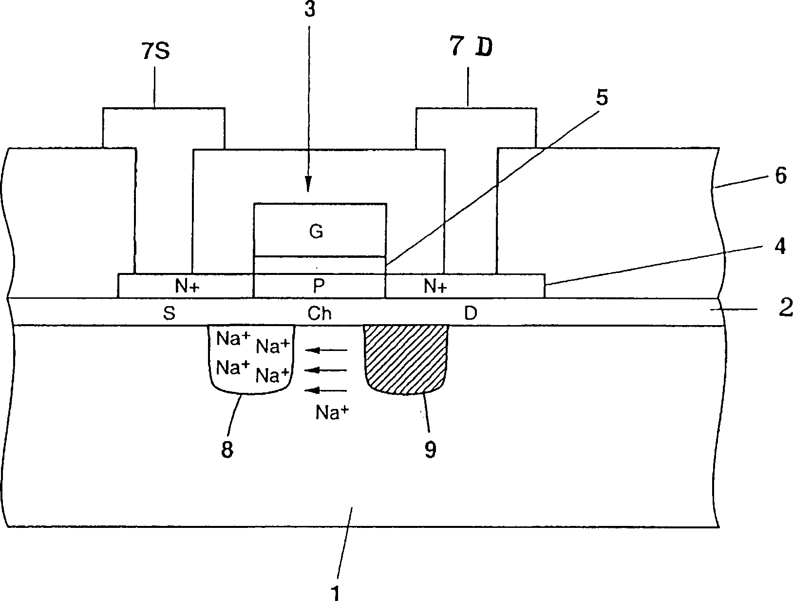
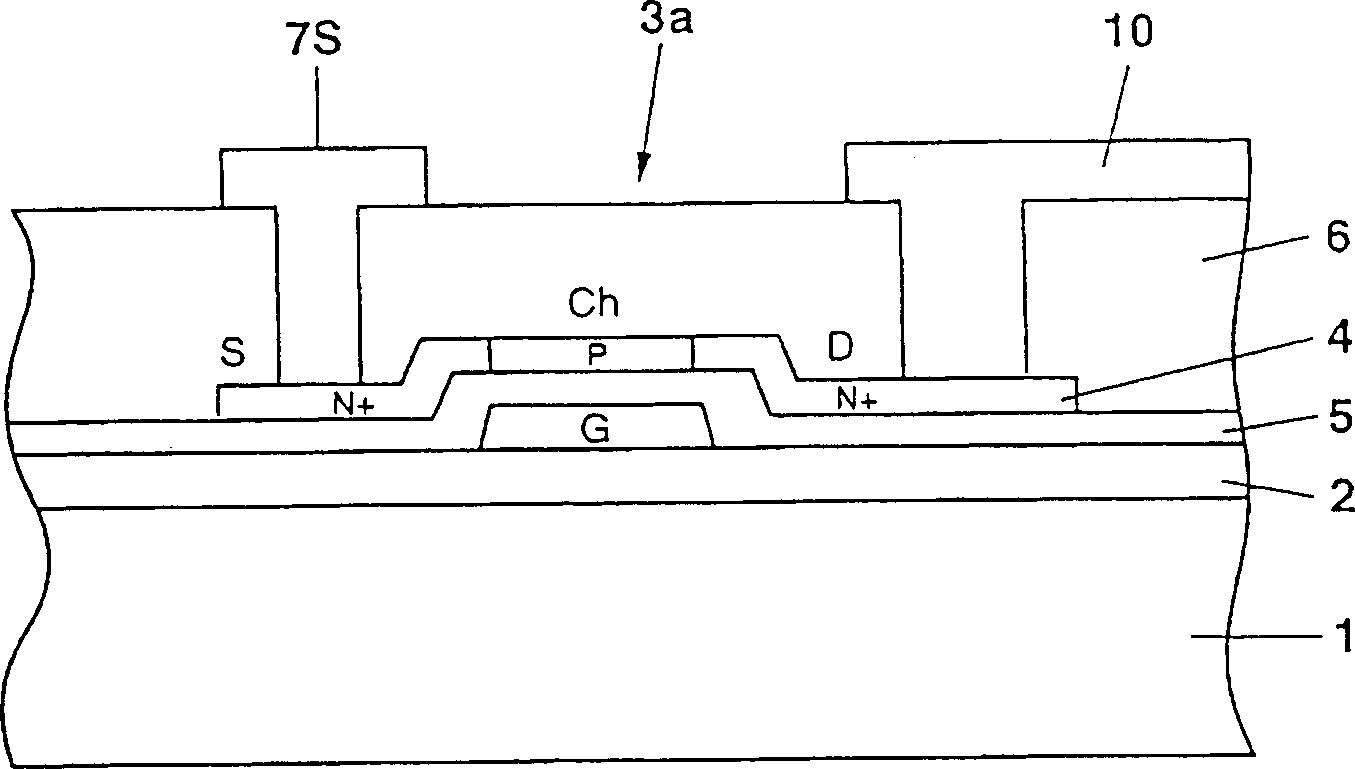
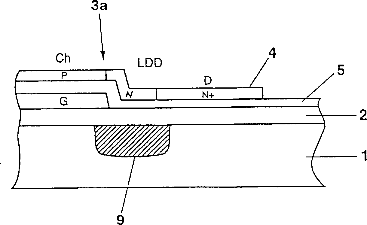
[0012] The best mode for carrying out the present invention will be described in detail with reference to the accompanying drawings. 1 shows a first preferred embodiment of a thin film semiconductor device according to the present invention, and is an example, in which an N-channel, top gate structure thin film transistor is formed on a glass substrate. As shown in FIG. 1, this thin film semiconductor device is formed using a glass substrate 1 containing an alkali metal such as sodium. The upper surface of the glass substrate 1 is covered with a buffer layer 2 . A thin film transistor 3 is formed on the buffer layer 2 . The thin film transistor 3 is a field effect transistor having a polycrystalline semiconductor thin film 4 containing polysilicon or the like as an active layer. The thin film transistor 3 has a top gate structure, and a gate electrode G is formed on the gate insulating layer 5 on the polycrystalline semiconductor film 4 through a mask. As a result, the chan...


PUM


Abstract

A thin film semiconductor device formed on a glass substrate that can improve the working characteristics and reliability of a thin film transistor. The thin film semiconductor device has a thin film transistor 3 formed on a glass substrate 1 containing an alkali metal. The glass substrate 1 is covered with a buffer layer 2 . The thin film transistor 3 formed on this buffer layer 2 has a polycrystalline semiconductor thin film 4 as an active layer. The buffer layer 2 includes at least one silicon nitride layer, and can prevent the thin film transistor 3 from being contaminated by an alkaline metal such as Na, and has such a thickness that it can protect the thin film transistor 3 from locally concentrated alkaline metal ions ( Na + ) of the electric field generated.

Description

technical field [0001] The invention relates to a thin-film semiconductor device used as a driving substrate of an active matrix liquid crystal display or a similar structure, in particular to a thin-film semiconductor device that uses ordinary glass as a substrate and is manufactured by a low-temperature process. In particular, it also relates to techniques for preventing the harmful effects of alkali metals contained in glasses. Background technique [0002] Thin film semiconductor devices are devices in which thin film transistors are formed on insulating substrates, and they have been greatly developed in recent years because they are ideal for application to driving substrates such as active matrix liquid crystal displays. Especially when using thin-film semiconductor devices in large-area liquid crystal displays. Necessary to reduce the cost of insulating substrates, glass substrates are used instead of the relatively high quality quartz substrates used in the past. ...

Claims


Application Information

Patent Timeline
Patent Type & Authority Patents(China)
IPC IPC(8): H01L29/786
CPCH01L29/78603H01L29/78606H01L27/12
Inventor 林久雄下垣内康加藤庆二
Owner JAPAN DISPLAY INC
Why Eureka
Try Eureka