Impedance matching method, impedance matcher and semiconductor process equipment

An impedance matcher and impedance matching technology, applied in discharge tubes, electrical components, circuits, etc., can solve problems such as process matching path differences, wafer process results, and matching time differences, so as to improve consistency and achieve fine adjustment. , improve the effect of repeatability and stability

Active Publication Date: 2021-01-22
BEIJING NAURA MICROELECTRONICS EQUIP CO LTD
View PDF5 Cites 1 Cited by
  • Summary
  • Abstract
  • Description
  • Claims
  • Application Information

AI Technical Summary

Problems solved by technology

[0005] However, in the above-mentioned matching process, especially for ICP (Inductively Coupled Plasma, Inductively Coupled Plasma), since the plasma is in the E-H mode transition (that is, from E mode to H mode) in the ignition process Steady state, resulting in differences and non-repeatability in the matching paths of different processes, resulting in differences in the matching time used by the processes for processing different wafers, which may cause different process results between wafers, especially for processes with shorter process times For this process, the difference in the results is more obvious

Method used


Image

  • Impedance matching method, impedance matcher and semiconductor process equipment
  • Impedance matching method, impedance matcher and semiconductor process equipment
  • Impedance matching method, impedance matcher and semiconductor process equipment

Examples


Embodiment Construction

[0039] In order for those skilled in the art to better understand the technical solution of the present invention, the impedance matching method, impedance matcher and semiconductor process equipment provided by the embodiments of the present invention applied to semiconductor process equipment will be described in detail below with reference to the accompanying drawings.

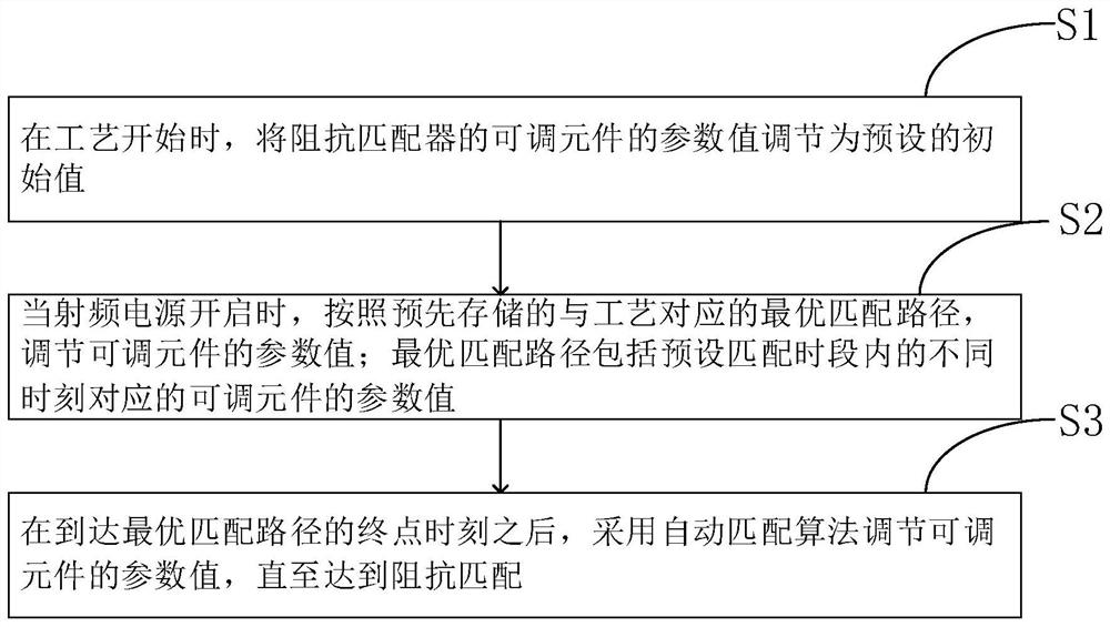
[0040] see figure 1 , the impedance matching method applied to semiconductor process equipment provided by the first embodiment of the present invention, which includes the following steps:

[0041] S1. At the beginning of the process, adjust the parameter value of the adjustable element of the impedance matching device to a preset initial value;

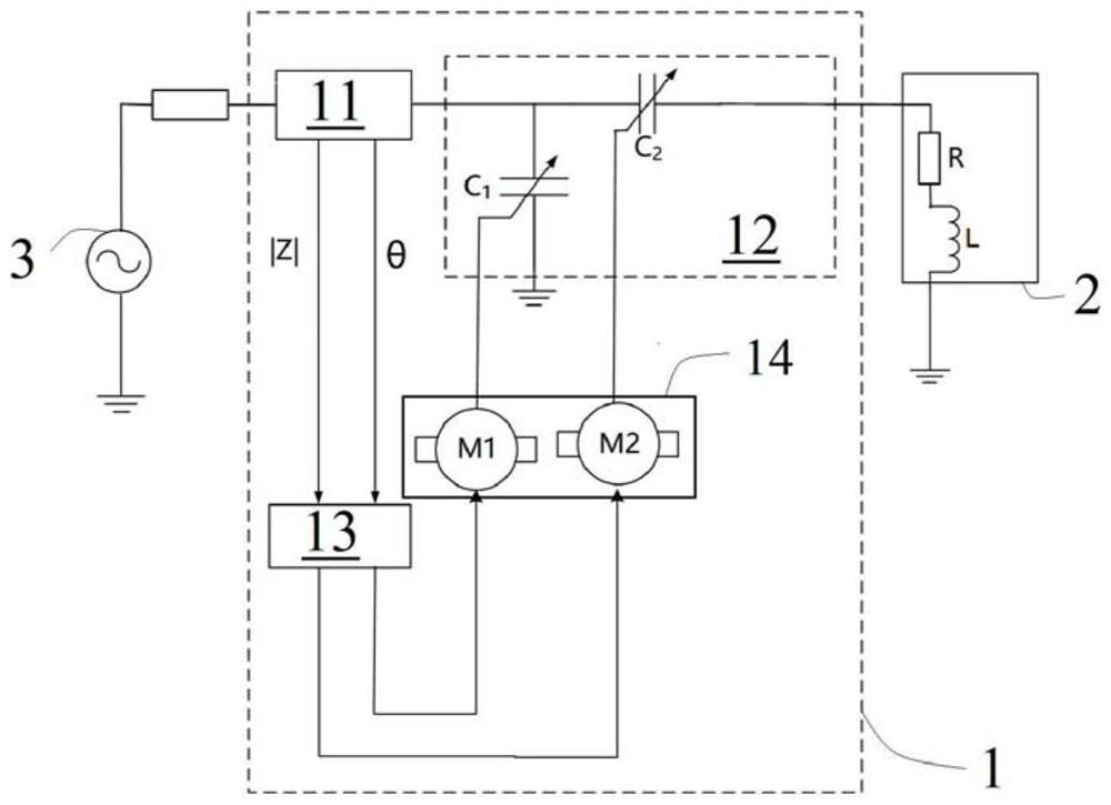
[0042] by figure 2 The impedance matching device 1 is shown as an example, the impedance matching device 1 is connected between the radio frequency power supply 3 and the process chamber 2, and is used to adjust the input impedance of the rear end of the radio ...


PUM


Abstract

The embodiment of the invention provides an impedance matching method and an impedance matcher applied to semiconductor process equipment, and the semiconductor process equipment. The impedance matching method comprises the following steps: at the beginning of a process, adjusting a parameter value of an adjustable element of an impedance matcher to a preset initial value; when a radio frequency power supply is turned on, adjusting the parameter value of the adjustable element according to a pre-stored optimal matching path corresponding to the process, wherein the optimal matching path comprises the parameter values, corresponding to different moments, of the adjustable element in a preset matching time period; and after the terminal point moment of the optimal matching path is reached, adjusting the parameter value of the adjustable element by adopting an automatic matching algorithm until impedance matching is achieved. According to the impedance matching method and the impedance matcher applied to the semiconductor process equipment, and the semiconductor process equipment provided by the embodiment of the invention, the repeatability and stability of the process can be improved, so that the consistency of process results can be improved.

Description

technical field [0001] The invention relates to the technical field of semiconductors, in particular to an impedance matching method applied to semiconductor process equipment, an impedance matcher and semiconductor process equipment. Background technique [0002] In the plasma processing equipment, the RF power supply transmits the RF energy to the process chamber through the impedance matching device, so as to excite the process gas in the process chamber to form plasma. The excited plasma contains a large number of electrons, ions, excitation These active particles interact with the wafer to cause various physical and chemical reactions on the surface of the wafer material, thereby completing the process of wafer etching or deposition. [0003] In the process of RF energy transmission, since the output impedance of the RF power supply is generally 50 ohms, the input impedance of the process chamber is generally a non-50 ohm impedance value with real part impedance and ima...

Claims


Application Information

Patent Timeline
Patent Type & Authority Applications(China)
IPC IPC(8): H01J37/32
CPCH01J37/32183H03H7/38H01J2237/3321H01J2237/334
Inventor 卫晶陈星韦刚华跃平
Owner BEIJING NAURA MICROELECTRONICS EQUIP CO LTD
Why Eureka
Try Eureka