Preparation method of heterojunction photodetector and photodetector

A photodetector and heterojunction technology, applied in semiconductor devices, final product manufacturing, sustainable manufacturing/processing, etc., can solve the problem of high detectable power (sensitivity), inability of detectors to perform detection, and inability to guarantee high-precision detection Requirements and other issues, to achieve flexible setting methods, achieve flexibility and scale, and reduce thresholds and costs

Active Publication Date: 2021-01-22
武汉敏芯半导体股份有限公司
View PDF4 Cites 0 Cited by
  • Summary
  • Abstract
  • Description
  • Claims
  • Application Information

AI Technical Summary

Problems solved by technology
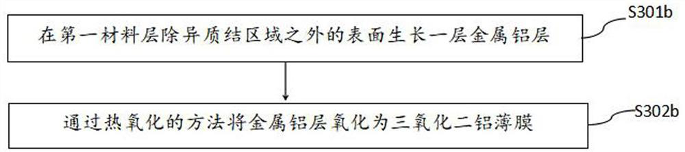
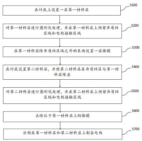
Therefore, the detector based on this mechanism cannot perform detection under zero bias voltage, and the dark current of the detector is not small, and the minimum detectable power (sensitivity) is large, which cannot guarantee high-end communications such as lidar, quantum communication, and atmospheric optical communication. Backhaul small signal detection in the link and other high-precision detection requirements

Method used


Image

  • Preparation method of heterojunction photodetector and photodetector
  • Preparation method of heterojunction photodetector and photodetector
  • Preparation method of heterojunction photodetector and photodetector

Examples


Embodiment Construction

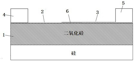
[0045] In describing the present invention, it should be understood that the terms "center", "longitudinal", "transverse", "length", "width", "thickness", "upper", "lower", "front", " Orientation or position indicated by "back", "left", "right", "vertical", "horizontal", "top", "bottom", "inner", "outer", "clockwise", "counterclockwise", etc. The relationship is based on the orientation or positional relationship shown in the drawings, and is only for the convenience of describing the present invention and simplifying the description, rather than indicating or implying that the referred device or element must have a specific orientation, be constructed and operated in a specific orientation, therefore It should not be construed as a limitation of the present invention.

[0046] In addition, the terms "first" and "second" are used for descriptive purposes only, and cannot be interpreted as indicating or implying relative importance or implicitly specifying the quantity of indic...


PUM

PropertyMeasurementUnit
thicknessaaaaaaaaaa

Abstract

The invention discloses a preparation method of a heterojunction photodetector and the photodetector. The preparation method comprises the steps of: setting a mask on a first material layer after graphical processing, and enabling the mask to cover the surface, except a heterojunction region, of the first material layer; and then setting a second material layer on a substrate, and stacking the second material layer with the first material layer in the heterojunction region. Therefore, the setting method of the second material layer on the substrate is more flexible, the stacking of the two materials by organic matter-assisted stripping and transferring in the prior art is avoided, and when the second material layer is subjected to graphical processing, the mask protects the first materiallayer, so that the preparation method of the heterojunction photodetector provided by the invention can realize the flexibility and the scale of the preparation of the low-dimensional material heterojunction, the preparation of the heterojunction is compatible with the CMOS process, and the threshold and the cost of the industrial preparation of the heterojunction are reduced.

Description

technical field [0001] The invention belongs to the technical field of photodetectors, and in particular relates to a preparation method of a heterojunction photodetector and the photodetector. Background technique [0002] Low-dimensional materials have become an important support for the development of a new generation of high-performance optoelectronic devices due to their outstanding optoelectronic properties, ultra-high carrier mobility, and excellent mechanical strength. They have application potential that cannot be achieved by traditional bulk materials. However, a single low-dimensional material still cannot meet the needs of multifunctional devices in practical applications. Therefore, the idea of ​​assembling different low-dimensional materials into van der Waals heterostructures to further improve device performance has emerged as the times require. Compared with traditional semiconductor heterojunctions, van der Waals heterojunctions are no longer limited by the...

Claims


Application Information

Patent Timeline
Patent Type & Authority Applications(China)
IPC IPC(8): H01L31/18H01L31/109
CPCH01L31/109H01L31/18Y02P70/50
Inventor 刘应军王权兵阳红涛王任凡
Owner 武汉敏芯半导体股份有限公司
Why Eureka
Try Eureka