
Semiconductor packaging device, light-emitting device and manufacturing method of semiconductor integrated circuit

A technology for packaging devices and integrated circuits, which is applied in the direction of semiconductor devices, printed circuit manufacturing, and electrical component assembly of printed circuits, etc., can solve the problems of low reliability of semiconductor packaging devices and insufficient processing solutions, etc., so as to facilitate popularization and use, improve reliability effect

Pending Publication Date: 2021-01-22
SHENZHEN JUFEI OPTOELECTRONICS
View PDF0 Cites 0 Cited by
  • Summary
  • Abstract
  • Description
  • Claims
  • Application Information

AI Technical Summary

Problems solved by technology

[0003] The manufacturing method of the semiconductor packaging device, the light-emitting device and the semiconductor integrated circuit provided by the present invention mainly solves the technical problem that: in the prior art, there are deficiencies in the air treatment scheme in the process of reflow soldering, resulting in low reliability of the semiconductor packaging device

Method used


Image

  • Semiconductor packaging device, light-emitting device and manufacturing method of semiconductor integrated circuit
  • Semiconductor packaging device, light-emitting device and manufacturing method of semiconductor integrated circuit
  • Semiconductor packaging device, light-emitting device and manufacturing method of semiconductor integrated circuit

Examples


Embodiment 1

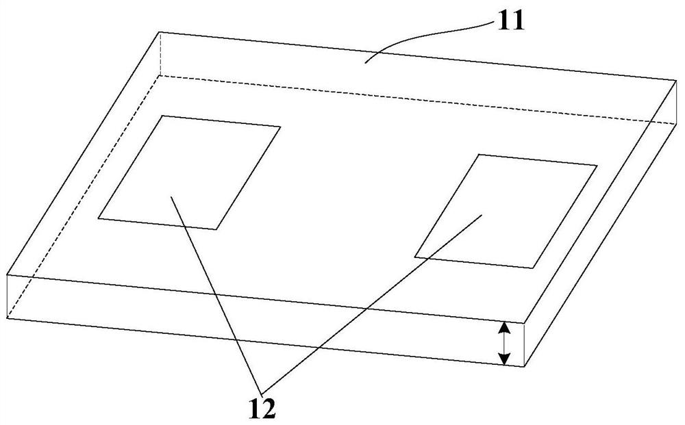
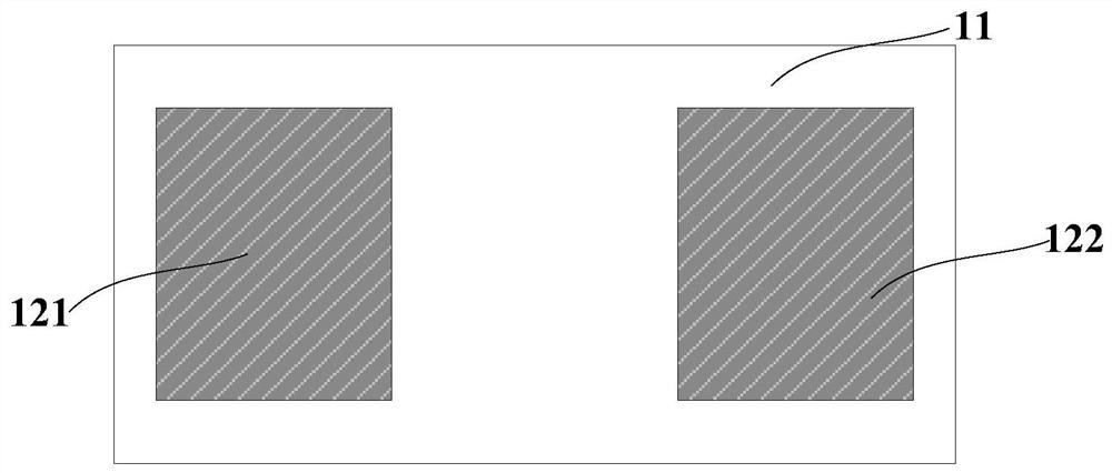
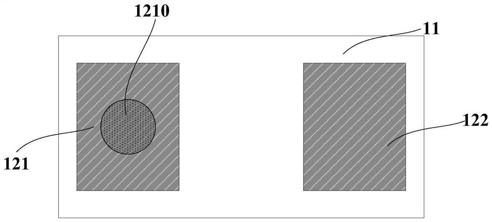
[0049] In order to solve the problem of insufficient air treatment solutions in the reflow soldering process in the prior art, resulting in low reliability of the semiconductor packaging device, this embodiment provides a semiconductor packaging device, the semiconductor packaging device includes a base, wherein, The base is composed of a non-metallic substrate and a metal pad, the metal pad penetrates the non-metallic substrate along the height direction, and at least one vent hole is provided on the metal pad, and the vent hole is used to discharge the air inside the semiconductor packaging device.

[0050] In this example, see Picture 1-1 , Figure 1-2 As shown, the metal pad 12 includes a first metal pad 121 and a second metal pad 122, and the first metal pad 121 and the second metal pad 122 respectively pass through the non-metal On the substrate 11 , the first metal pad 121 is isolated from the second metal pad 122 by the non-metallic substrate 11 .

[0051] The first ...

Embodiment 2

[0085] In order to solve the problem of insufficient air treatment solutions in the reflow soldering process in the prior art, resulting in low reliability of semiconductor packaging devices, this embodiment provides a method for manufacturing a semiconductor integrated circuit. Please refer to Figure 4 As shown, the manufacturing method of the semiconductor integrated circuit includes:

[0086] S401: Use the steel mesh as a mold to print soldering material on the PCB circuit board;

[0087] S402: Attach the semiconductor package device with vent holes on the pad to the corresponding soldering material position on the PCB circuit board;

[0088] S403: Place the PCB circuit board on which the semiconductor packaging device has been attached in S402 in the reflow furnace for reflow heating. During the heating process of the reflow furnace, the air inside the semiconductor packaging device is discharged from the vent hole of the pad at the bottom of the bowl, and at the same tim...

Embodiment 3

[0121] This embodiment also provides a light emitting device, which includes the semiconductor packaging device exemplified in the above embodiments. The light emitting device in this embodiment may be an illuminating device, a light signal indicating device, a supplementary light device or a backlight device, and the like. When it is a lighting device, it can specifically be a lighting device used in various fields, such as desk lamps, fluorescent lamps, ceiling lamps, downlights, street lights, projection lights, etc. in daily life, and for example, high beams and low beams in cars Lamps, ambient lights, etc., such as surgical lights, low-electromagnetic lighting, and lighting for various medical instruments, and various colored lights, landscape lighting, advertising lights, etc. in the field of decorative lighting; for In the case of an optical signal indicating device, it may specifically be an optical signal indicating device applied in various fields, such as signal ind...


PUM


Abstract

The invention provides a semiconductor packaging device, a light-emitting device and a manufacturing method of a semiconductor integrated circuit. Air in the semiconductor packaging device is exhausted from an exhaust hole formed in a bonding pad at the bottom of a bowl cup of the semiconductor packaging device in a heating process of a reflow oven; meanwhile, the welding material is molten and gradually infiltrates the exhaust hole of the bonding pad at the bottom of the bowl cup, so that the molten welding material of the bonding pad at the bottom of the bowl cup is gradually cooled and condensed into solid metal to seal the exhaust hole, thereby avoiding the phenomenon that the performance of the semiconductor packaging device is influenced due to the fact that an organic filler in thesemiconductor packaging device is easy to age; the reliability of the semiconductor packaging device is improved; and the semiconductor packaging device is always in a closed state after internal airis exhausted, so that external environmental pollutants cannot enter the semiconductor packaging device, the reliability of the semiconductor packaging device is further improved, the semiconductor packaging device can be better suitable for application scenes of various environments, and popularization and application are facilitated.

Description

technical field [0001] The present invention relates to the field of LED (Light Emitting Diode, light emitting diode), in particular to a semiconductor packaging device, a light emitting device and a manufacturing method of a semiconductor integrated circuit. Background technique [0002] At present, the installation and soldering of semiconductor packaging devices generally adopts the method of reflow soldering, in which the reflow soldering temperature will exceed 230°C. If there is a large amount of air inside the semiconductor packaging device, the air will expand rapidly as the temperature rises during the reflow soldering process, causing damage to the device. In order to avoid this phenomenon, the existing semiconductor packaging device adopts a solution of filling organic material in the internal space of the device to discharge or reduce the air inside the device. However, this solution has certain limitations. The internal organic filler has poor environmental adap...

Claims


Application Information

Patent Timeline
Patent Type & Authority Applications(China)
IPC IPC(8): H01L33/62H01L33/48H05K3/34
CPCH01L33/486H01L33/62H05K3/341H01L2933/0033H01L2933/0066
Inventor 张志宽高丹鹏邢美正
Owner SHENZHEN JUFEI OPTOELECTRONICS
Learn More