A kind of arrayed waveguide grating with double-layer structure

A technology of arrayed waveguide grating and double-layer structure, which is applied in the direction of optical waveguide light guide, optics, light guide, etc., can solve the problems of large device size, high insertion loss, high crosstalk, etc., and achieve the effect of reducing size

Active Publication Date: 2022-04-19
ZHEJIANG UNIV
View PDF7 Cites 0 Cited by
  • Summary
  • Abstract
  • Description
  • Claims
  • Application Information

AI Technical Summary

Problems solved by technology

[0003] Arrayed waveguide gratings are key devices for multiplexing / demultiplexing and wavelength routing functions in WDM systems. Common array waveguide gratings (array waveguide gratings, AWGs) include silicon dioxide and silicon-based AWGs, which represent low-refractive index-based The AWG of the differential waveguide and the AWG based on the high refractive index difference waveguide, although the AWG based on the high refractive index difference waveguide benefits from the nanoscale waveguide size and the micron-scale bending radius, it can achieve a very small device size, but the disadvantage is that it needs to Guaranteeing the working performance of AWG requires very high resolution fabrication technology, usually with high insertion loss and high crosstalk
Based on the AWG with low relative refractive index difference, although the device performance is very good, the fatal thing is that the device size is very large, even reaching the centimeter level.

Method used


Image

  • A kind of arrayed waveguide grating with double-layer structure
  • A kind of arrayed waveguide grating with double-layer structure
  • A kind of arrayed waveguide grating with double-layer structure

Examples


Embodiment Construction

[0029] The present invention will now be further described in conjunction with the accompanying drawings and specific embodiments.

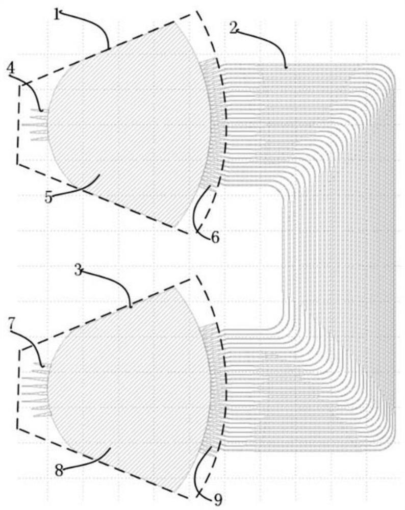
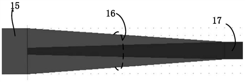
[0030] Such as figure 1 It is a double-layer arrayed waveguide grating of the present invention, including an input star coupler 1, an array waveguide 2, and an output star coupler 3; the input star coupler 1 includes an input channel waveguide 4, an input slab waveguide 5. Input transition waveguide 6; the output star coupler 3 includes an output channel waveguide 7, an output slab waveguide 8, and an output transition waveguide 9; the output channel waveguide 7 includes a second single-mode waveguide part 13, a second taper transition Structure 14 (with Figure 3B The waveguide structure of the input channel that can realize the common sinusoidal spectral response is the same);

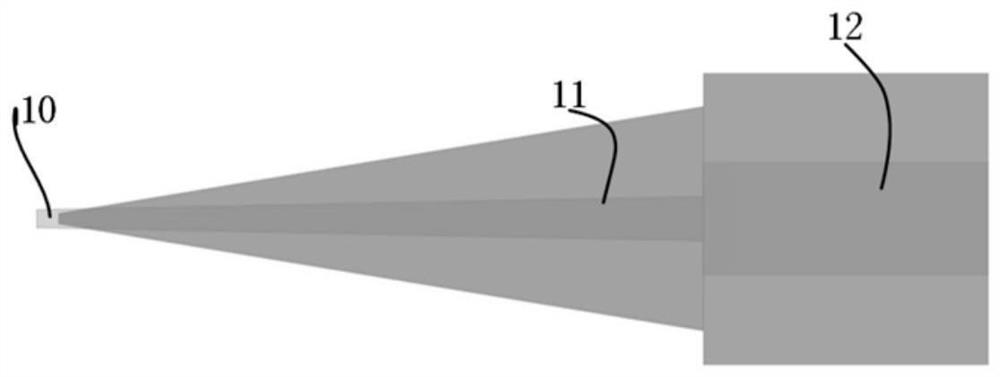
[0031] In order to reduce the scattering loss caused by the mode mismatch between the slab waveguide and the array waveguide, the array waveguide 2 is respectively c...


PUM


Abstract

The invention discloses an arrayed waveguide grating with a double-layer structure. The arrayed waveguide grating includes an input star coupler (including an input channel waveguide, an input slab waveguide and an input transition waveguide), an array waveguide and an output star coupler ( Including the output channel waveguide, the output slab waveguide and the output transition waveguide, the array waveguide is respectively connected with the input star coupler and the output star coupler to reduce the scattering loss by the input transition waveguide and the output transition waveguide. The double-layer structure of the present invention Compared with the traditional single-layer AWG, AWG combines the advantages of strong confinement waveguide (Δ>25%) and weak confinement waveguide (Δ<25%), which is expected to reduce the size of the device while ensuring the performance of AWG devices , which provides feasibility for on-chip integration and commercialization of AWG devices.

Description

technical field [0001] The invention belongs to the field of wavelength division multiplexing application systems in optical fiber communication, and in particular relates to a double-layer arrayed waveguide grating. Background technique [0002] Nowadays, optical communication systems have been widely used, and in order to maximize the communication capacity of optical fiber systems, wavelength division multiplexing (WDM) systems using multi-carrier wavelengths emerged as the times require. The key device in the WDM system is the wavelength multiplexer / demultiplexer. A multiplexer combines all wavelength channels on a single fiber, while a demultiplexer separates wavelengths from a single fiber into multiple wavelength channels. [0003] Arrayed waveguide gratings are key devices for multiplexing / demultiplexing and wavelength routing functions in WDM systems. Common array waveguide gratings (array waveguide gratings, AWGs) include silicon dioxide and silicon-based AWGs, wh...

Claims


Application Information

Patent Timeline
Patent Type & Authority Patents(China)
IPC IPC(8): G02B6/12
CPCG02B6/12009G02B2006/12147
Inventor 宁楠楠王肖飞余辉杨建义王曰海
Owner ZHEJIANG UNIV
Why Eureka
Try Eureka