Display substrate and production method thereof, and display device

A display substrate and substrate technology, applied in semiconductor/solid-state device manufacturing, electrical components, electrical solid-state devices, etc., can solve problems such as packaging film interface peeling, reduce stress mismatch, ensure reliability, and reduce adhesion The effect of difference

Inactive Publication Date: 2021-02-02
BOE TECH GRP CO LTD
View PDF5 Cites 1 Cited by
  • Summary
  • Abstract
  • Description
  • Claims
  • Application Information

AI Technical Summary

Problems solved by technology

[0006] The technical problem to be solved by the present disclosure is to provide a display substrate and its preparation method, and a display device, so as to solve the problems of interface peeling in the existing packaging film layer.

Method used


Image

  • Display substrate and production method thereof, and display device
  • Display substrate and production method thereof, and display device
  • Display substrate and production method thereof, and display device

Examples


Embodiment approach

[0193] The present disclosure also provides a method for preparing the display substrate. In an exemplary embodiment, the preparation method includes:

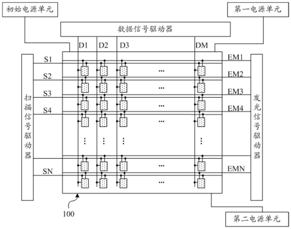
[0194] S1, forming a light-emitting structure layer on the substrate;

[0195] S2. Form an encapsulation structure layer on the light emitting structure layer, the encapsulation structure layer includes an encapsulation layer and at least one transition layer, the side of the transition layer adjacent to the substrate is in contact with the first side film layer, and the transition layer The side of the layer away from the substrate is in contact with the second side film layer, and the adhesion of the at least one transition layer is greater than the adhesion of one of the first side film layer and the second side film layer, and less than Adhesion of the other film layer in the first side film layer and the second side film layer.

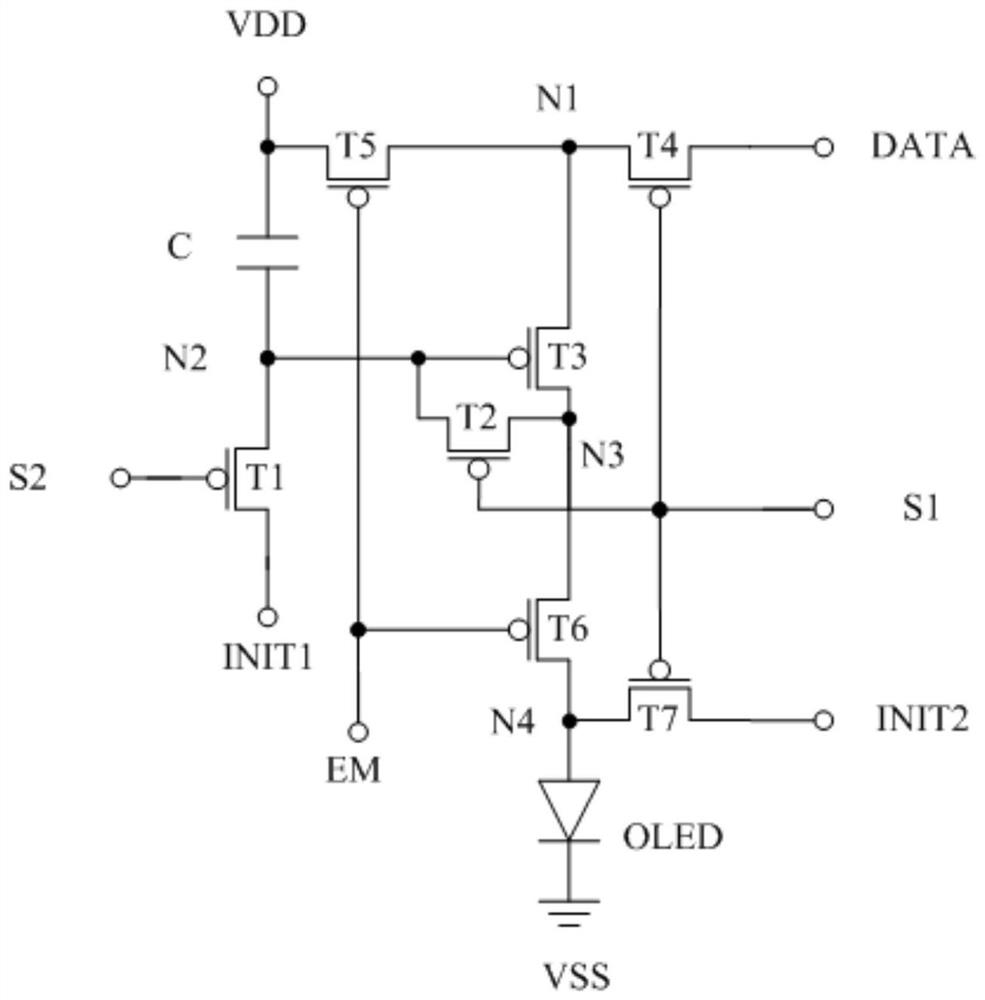
[0196] In an exemplary embodiment, the light emitting structure layer may include a driving...


PUM

PropertyMeasurementUnit
thicknessaaaaaaaaaa
adhesivityaaaaaaaaaa

Abstract

The invention provides a display substrate and a production method thereof, and a display device. The display substrate comprises a substrate body, a light-emitting structure layer arranged on the substrate body and a packaging structure layer arranged on the light-emitting structure layer. The packaging structure layer comprises a packaging layer and at least one transition layer, the side, adjacent to the substrate body, of the transition layer makes contact with a first side film layer, the side, away from the substrate body, of the transition layer makes contact with a second side film layer, and an adhesive force of the at least one transition layer is larger than that of one of the first side film layer and the second side film layer. And the adhesive force is smaller than that of the other one of the first side film layer and the second side film layer. Through the arrangement of the transition layer, an adhesive force difference between the film layers is reduced, the stress mismatching between the film layers is reduced, interface stripping between the film layers is effectively avoided, the reliability of film packaging is ensured, the reliability of film packaging can begreatly improved, and bending resistance and a curling capacity of the display substrate can be greatly increased.

Description

technical field [0001] The present disclosure relates to but is not limited to the field of display technology, especially to a display substrate, a manufacturing method thereof, and a display device. Background technique [0002] Organic Light Emitting Diode (OLED) is an active light-emitting display device, which has the advantages of self-illumination, wide viewing angle, high contrast, low power consumption, high response speed, light and thin, bendable and low cost. With the continuous development of display technology, a flexible display device (Flexible Display) which uses OLED as a light-emitting device and is signal-controlled by a Thin Film Transistor (TFT) has become a mainstream product in the display field. [0003] Because the water and oxygen in the outside air invade the light-emitting device, the organic light-emitting material will be eroded by water and oxygen, and an oxidation reaction will occur, causing the pixel to shrink or not emit light, the perform...

Claims


Application Information

Patent Timeline
Patent Type & Authority Applications(China)
IPC IPC(8): H01L51/52H01L51/56H01L27/32
CPCH10K59/12H10K50/844H10K71/00
Inventor 王涛孙韬秦成杰张子予张嵩王有为洪瑞
Owner BOE TECH GRP CO LTD
Why Eureka
Try Eureka