
Same-frequency LED lighting source construction method for detecting product surface two-dimensional defects

A technology of LED lighting and construction method, applied in the direction of optical testing flaws/defects, etc., can solve the problems of insufficient bright spots and poor heat dissipation of the lighting source, and achieve the effect of good lighting effect, meeting lighting needs and good application prospects.

Active Publication Date: 2021-02-05
江苏善果缘智能科技有限公司
View PDF5 Cites 0 Cited by
  • Summary
  • Abstract
  • Description
  • Claims
  • Application Information

AI Technical Summary

Problems solved by technology

[0007] The purpose of the present invention is to overcome the problems of insufficient bright spots of the lighting source and poor heat dissipation during the scanning and sampling process of the CCD sensor for the detection of product surface defects.

Method used


Image

  • Same-frequency LED lighting source construction method for detecting product surface two-dimensional defects
  • Same-frequency LED lighting source construction method for detecting product surface two-dimensional defects

Examples


Embodiment Construction

[0034] The present invention will be further described below in conjunction with the accompanying drawings.

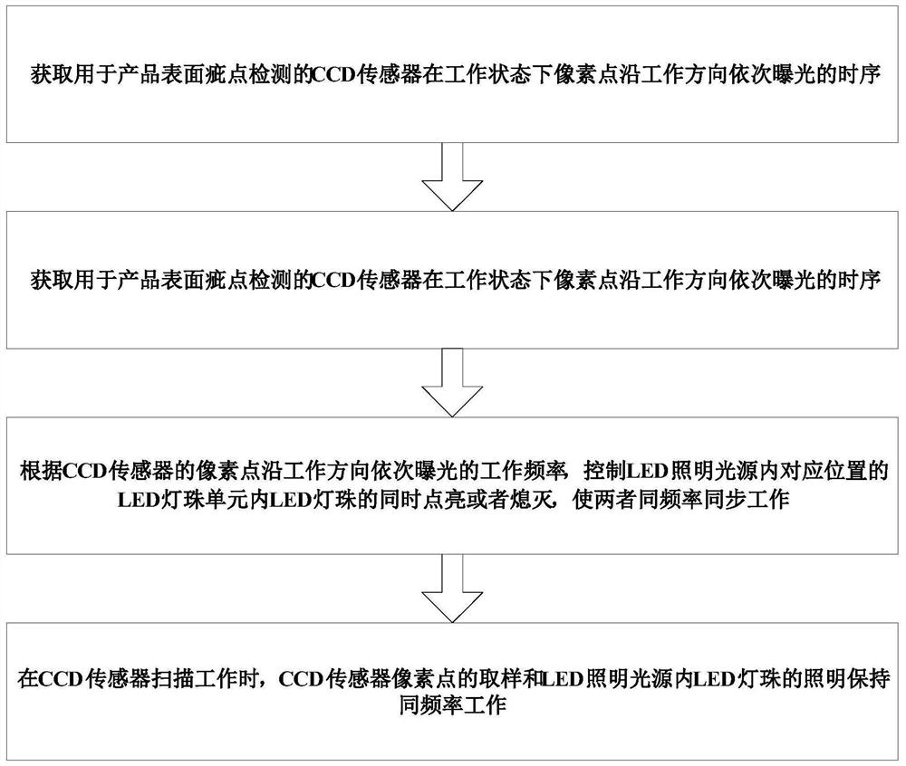
[0035] Such as figure 1 As shown, the construction method of the same-frequency confocal LED lighting source for CCD sensor scanning of the present invention comprises the following steps,

[0036] Step (A), obtaining the time sequence of sequentially exposing pixels along the working direction of the CCD sensor used for product surface defect detection in the working state, includes the following steps,

[0037] (A1), connect the electrical signal test instrument with the CCD sensor, and establish a test environment;

[0038] (A2), provide the required clock signal and power supply to the CCD sensor to make it work normally;

[0039] (A3), sequentially perform instantaneous single-point illumination on each pixel point in the CCD sensor that is working normally, and record the output signal of the pixel point of the CCD sensor through the electrical signal tester, a...


PUM


Abstract

The invention discloses a same-frequency LED lighting source construction method for detecting product surface two-dimensional defects. The same-frequency LED lighting source construction method is characterized by selecting a same-frequency LED lighting source for lighting according to attributive characteristics of the product surface two-dimensional defects, facilitating detection of the two-dimensional defects including different colors, stains and damages, and enabling the LED lighting sources to instantaneously lighten LED lamp beads. According to the working property that the LED lighting sources can be lightened individually, the LED lamp beads at the corresponding positions are lightened in a mapping control mode, overload can be ensured, the brightness is remarkably improved, anddue to the fact that the power-on time is short, the actual power consumption is low, the heating amount is small, an active heat dissipation component is not needed any more, the overall size is small, field installation of product surface detection is facilitated, pixels of a CCD sensor are synchronously lightened in sequence, the service life is prolonged, the illumination effect is good, theheat dissipation efficiency is high, the accuracy of detection and sampling of the product surface two-dimensional defects is greatly improved, and the same-frequency LED lighting source constructionmethod has good application prospect while the illumination requirement is met.

Description

technical field [0001] The invention relates to the technical field of product surface detection, in particular to a method for constructing a same-frequency LED lighting source for two-dimensional defect detection on the product surface. Background technique [0002] CCD sensor, made of a high-sensitivity semiconductor material, can convert light into electric charge, and convert it into digital signal through analog-to-digital converter for computer to process it. At present, CCD sensors have been widely used in the detection of surface defects of industrial products. Especially for the detection of various defects on the product surface. [0003] In the detection process of product surface defects (with high precision requirements), the sampling environment is very important, and reliable and high-precision data must be provided for the subsequent image processing process to obtain accurate defect detection results. [0004] In the prior art, for the detection of two-di...

Claims


Application Information

Patent Timeline
Patent Type & Authority Applications(China)
IPC IPC(8): G01N21/88G01N21/94
CPCG01N21/88G01N21/94Y02B20/40
Inventor 周维郑步笑徐存辉陈立新
Owner 江苏善果缘智能科技有限公司
Learn More