

Panchromatic Micro/Nano LED array direct epitaxy method and structure
An array and epitaxy technology, applied in electrical components, electrical solid-state devices, circuits, etc., can solve the problems of difficulty in independent addressing of a single drive and complex technology, reduce manufacturing difficulty and manufacturing cost, overcome process bottlenecks, and achieve ultra-high performance. The effect of high LED density
- Summary
- Abstract
- Description
- Claims
- Application Information
AI Technical Summary
Problems solved by technology
Method used
Image

Examples
Embodiment Construction
[0047] The present invention will be further described below through specific embodiments.
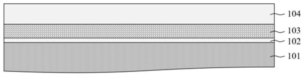
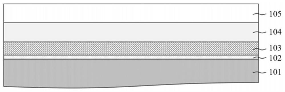
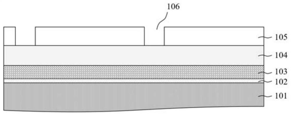
[0048] The present invention proposes a direct epitaxial structure of a full-color Micro / Nano LED array, including a bottom-up substrate 101, a buffer layer 102, an unintentionally doped layer 103, an n-type layer 104, and an array of LED light-emitting units. The LED light-emitting unit The array is a light-emitting unit of any color produced by a step-by-step selective area epitaxy method; it also includes an n-type electrode array and a p-type electrode array, the n-type electrode array is electrically connected to the n-type layer 104, and the p-type electrode array is connected to the light-emitting unit The p-type layer is electrically connected to realize independent addressing and driving. The structure of the present invention can realize the independent addressing and driving of each LED.
[0049] The present invention also proposes a direct epitaxial method of Micro / Nano fu...
PUM
| Property | Measurement | Unit |
|---|---|---|
| size | aaaaa | aaaaa |
| size | aaaaa | aaaaa |
| emission peak | aaaaa | aaaaa |
Abstract
Description
Claims
Application Information