Manufacturing method of shielded gate trench mosfet

A manufacturing method and shielding grid technology, which is applied in semiconductor/solid-state device manufacturing, semiconductor devices, electrical components, etc., can solve the problems of bound applications, increase gate-source leakage, and reduce gate-source leakage, so as to achieve low process cost and solve process bottleneck effect

Active Publication Date: 2019-01-04
SHANGHAI HUAHONG GRACE SEMICON MFG CORP
View PDF6 Cites 0 Cited by
  • Summary
  • Abstract
  • Description
  • Claims
  • Application Information

AI Technical Summary

Problems solved by technology

[0019] It can be seen from the above that the above-mentioned polysilicon gate with sidewall polysilicon structure is a deep trench gate MOSFET device with a separated side gate structure with a shielded gate, or a shielded gate trench MOSFET with a left and right structure, which is used in the existing formation process method Bottom-up process implementation approach, consisting of Figure 1G As shown, it can be seen that the gate oxide layer 106a and the isolation dielectric layer of the shield gate, that is, the polysilicon isolation dielectric layer 106b, are formed at the same time, so that the gate oxide layer 106a determines the gap between the deep trench gate, that is, the polysilicon gate 107, and the shield gate, that is, the source polysilicon 105. When the thickness of the gate oxide layer 106a is relatively thin, it is easy to cause leakage between the gate and the source, which restricts the application of this structure in devices with low threshold voltage or turn-on voltage.
It can be seen that in order to obtain a low threshold voltage device, a thinner gate oxide layer 106a is required, and a thinner gate oxide layer 106a will simultaneously reduce the thickness of the inter-polysilicon isolation dielectric layer 106b to increase the leakage between the gate and source , so the existing method cannot solve the contradiction between lowering the threshold voltage and reducing the gate-source leakage

Method used


Image

  • Manufacturing method of shielded gate trench mosfet
  • Manufacturing method of shielded gate trench mosfet
  • Manufacturing method of shielded gate trench mosfet

Examples


Embodiment Construction

[0050] Such as figure 2 Shown is the flow chart of the method of the embodiment of the present invention; Figure 3A to Figure 3K Shown is a schematic diagram of the device structure in each step of the method of the embodiment of the present invention. The gate structure of the manufacturing method of the shielded gate trench MOSFET according to the embodiment of the present invention is formed by the following steps:

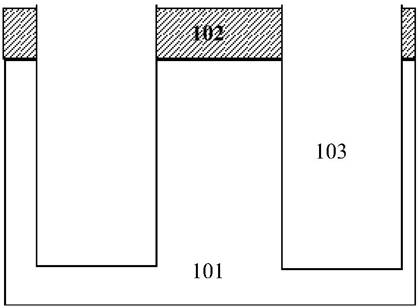
[0051] Step 1, such as Figure 3A As shown, a semiconductor substrate 1 is provided, a hard mask layer 201 is formed on the surface of the semiconductor substrate 1, a gate formation region is defined by a photolithography process, and the gate formation region is formed by an etching process. The hard mask layer 201 is removed.

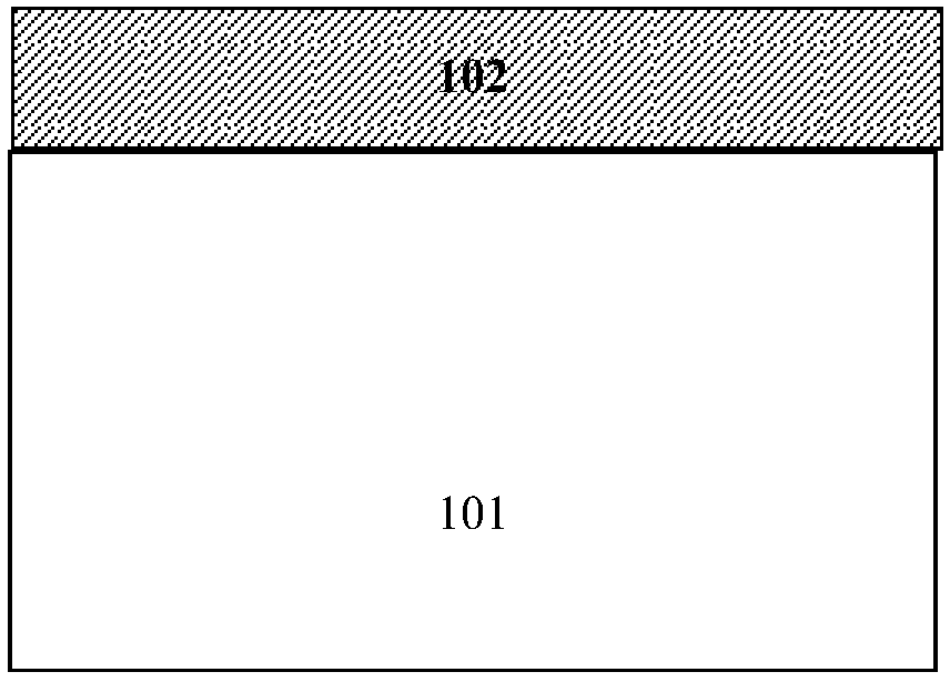
[0052] Preferably, the semiconductor substrate 1 is a silicon substrate, and a silicon epitaxial layer is formed on the surface of the silicon substrate 1 . The hard mask layer 201 is composed of an oxide layer.
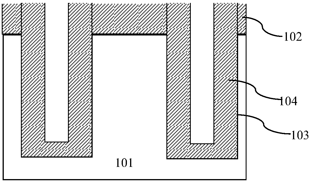
[0053] Step t...


PUM


Abstract

The invention discloses a method for manufacturing a shielded gate trench MOSFET. The gate structure is formed by the following steps: forming a hard mask layer and defining a gate forming region; etching a semiconductor substrate to form a deep trench; forming Bottom oxide layer; forming source polysilicon; performing polysilicon etching back to make the source polysilicon and the top surface of the hard mask layer level; removing the hard mask layer to form the top protruding structure of the source polysilicon; on the side of the protruding part of the source polysilicon Forming sidewalls composed of an oxide etch barrier layer; using the sidewalls as a self-aligned mask to etch the bottom oxide layer to form a top trench and an isolation oxide layer between polysilicon on both sides of the source polysilicon; in the top trench Form the gate dielectric layer on the sides; fill the top trench to form a polysilicon gate. The invention can reduce the gate-source leakage of the device while reducing the threshold voltage of the device.

Description

technical field [0001] The invention relates to a method for manufacturing a semiconductor integrated circuit, in particular to a method for manufacturing a shield gate (Shield Gate Trench, SGT) deep trench MOSFET. Background technique [0002] Such as Figure 1A to Figure 1N As shown, it is a schematic diagram of the device structure in each step of the manufacturing method of the existing shielded gate trench MOSFET; this method adopts a bottom-up method to form a deep trench separated side gate structure with a shielded gate, including the following steps: [0003] Step 1, such as Figure 1A As shown, a semiconductor substrate such as a silicon substrate 101 is provided; a hard mask layer 102 is formed on the surface of the semiconductor substrate 101, and the hard mask layer 102 can be an oxide layer, or an oxide layer plus a nitride layer. [0004] Such as Figure 1B As shown, the hard mask layer 102 is then etched by a photolithography process to define a gate format...

Claims


Application Information

Patent Timeline
Patent Type & Authority Patents(China)
IPC IPC(8): H01L21/336H01L29/78H01L21/28H01L29/423
CPCH01L29/401H01L29/42356H01L29/4236H01L29/42364H01L29/6656H01L29/66666H01L29/7827H01L29/407H01L29/7813H01L29/66734H01L29/41766
Inventor 颜树范
Owner SHANGHAI HUAHONG GRACE SEMICON MFG CORP
Why Eureka
Try Eureka