
Backside illuminated image sensor and forming method thereof

An image sensor, back-illuminated technology, applied in the direction of electric solid-state devices, semiconductor devices, electrical components, etc., can solve the problems of complex process, can not meet the miniaturization of back-illuminated image sensors, and the reduction of chip size.

Inactive Publication Date: 2021-02-09
WUHAN XINXIN SEMICON MFG CO LTD
View PDF5 Cites 0 Cited by
  • Summary
  • Abstract
  • Description
  • Claims
  • Application Information

AI Technical Summary

Problems solved by technology

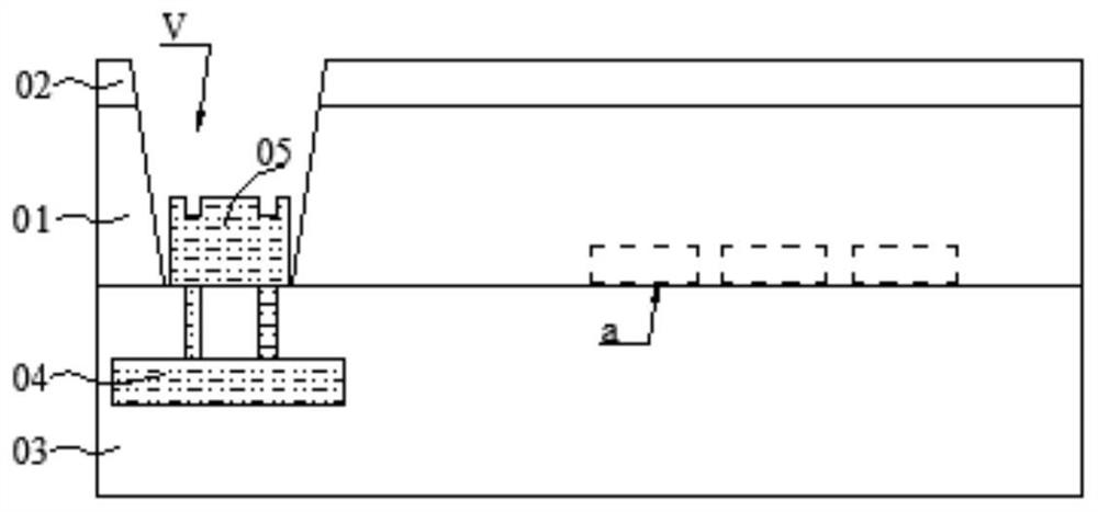
In order to form the bonding pad 05 in this backside lead method, it is necessary to form a large-area opening V on the substrate 01. Devices cannot be designed in the large-area opening V area on the substrate 01, and the chip area utilization rate is low. Limits the further reduction of the chip size of the back-illuminated image sensor, and cannot meet the miniaturization requirements of the back-illuminated image sensor
In addition, the back lead process and the trench isolation process are formed separately, using different masks, and formed in different etching steps, the process is more complicated

Method used


Image

  • Backside illuminated image sensor and forming method thereof
  • Backside illuminated image sensor and forming method thereof
  • Backside illuminated image sensor and forming method thereof

Examples


Embodiment Construction

[0033] Embodiments of the present invention provide a back-illuminated image sensor and a forming method thereof. The present invention will be described in further detail below in conjunction with the accompanying drawings and specific embodiments. The advantages and features of the present invention will become clearer from the following description. It should be noted that the drawings are all in a very simplified form and use imprecise scales, and are only used to facilitate and clearly assist the purpose of illustrating the embodiments of the present invention.

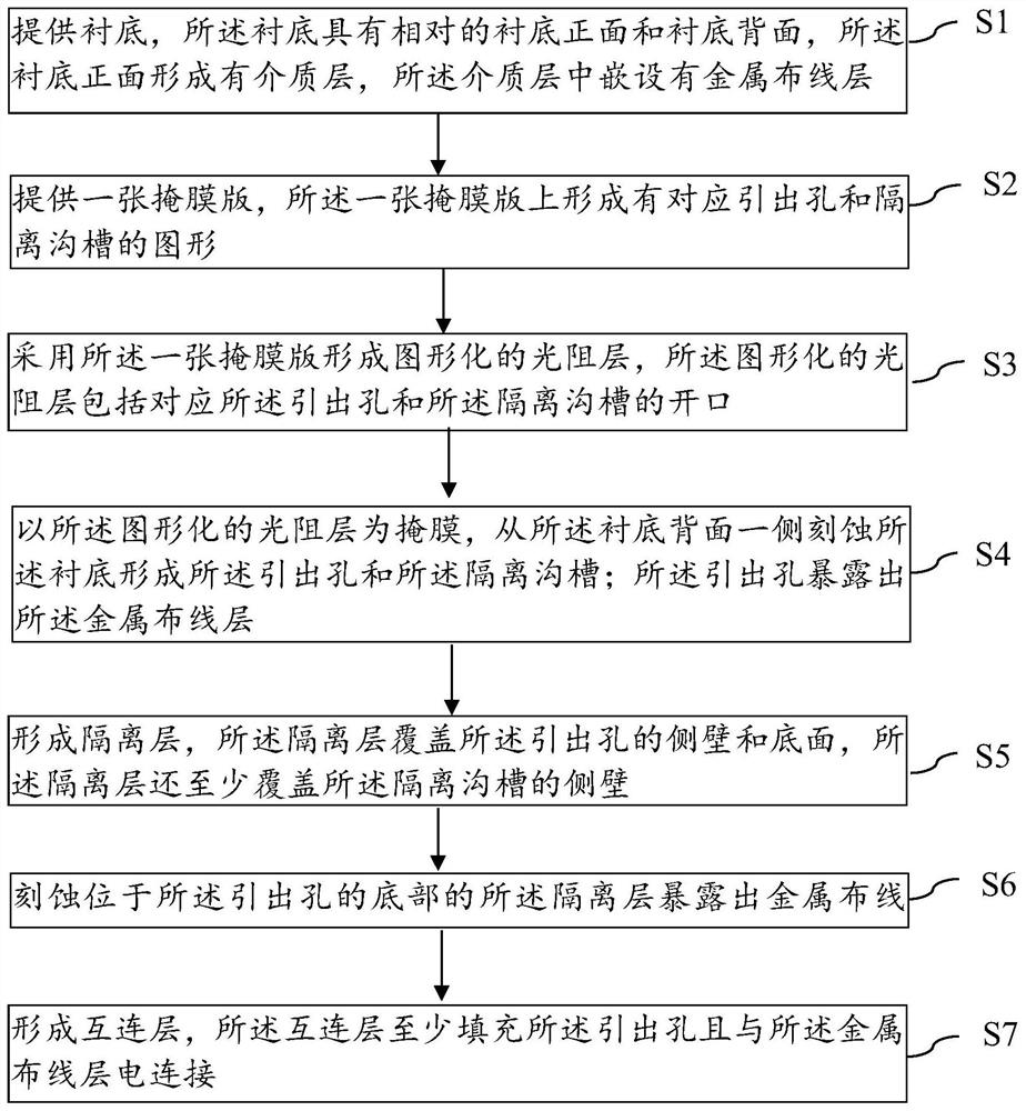
[0034] An embodiment of the present invention provides a method for forming a back-illuminated image sensor, such as figure 2 shown, including:

[0035] S1. Provide a substrate, the substrate has a substrate front and a substrate back opposite, a dielectric layer is formed on the substrate front, and a metal wiring layer is embedded in the dielectric layer;

[0036] S2. Provide a mask plate, and the pattern c...


PUM


Abstract

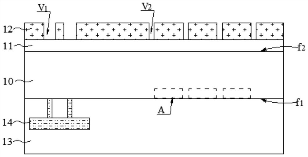
The invention provides a backside illuminated image sensor and a forming method thereof. The forming method comprises the following steps of providing a substrate; forming patterns corresponding to the lead-out holes and the isolation grooves on one mask plate; forming a graphical photoresist layer by adopting one mask plate, wherein the graphical photoresist layer comprises openings correspondingto the lead-out holes and the isolation grooves; etching the substrate from one side of the back surface of the substrate by taking the graphical photoresist layer as a mask to form the lead-out holes and the isolation grooves; forming an isolation layer, wherein the side wall of the isolation trench is at least covered by the isolation layer; and forming interconnect layers. According to the method, the hole area is reduced, and the chip area utilization rate is improved. According to the present invention, patterns corresponding to the lead-out holes and the isolation grooves are formed onone mask plate, the lead-out holes and the isolation grooves are formed at the same time through one etching process, a back lead process and a groove isolation process are carried out at the same time, the process is simplified, and the process cost is reduced; and the side wall of the isolation groove is at least covered by the isolation layer, so that the electrical isolation capability betweendifferent pixel units is improved.

Description

technical field [0001] The invention belongs to the technical field of integrated circuit manufacturing, and in particular relates to a back-illuminated image sensor and a forming method thereof. Background technique [0002] Back-illuminated image sensor (BSI) is currently the most widely used CMOS image sensor. Compared with front-illuminated image sensor (FSI), the process of BSI is characterized by flipping the wafer with pixel units through wafer bonding technology to realize The incident light is directly irradiated on the back of the silicon wafer without passing through the front dielectric layer and metal wiring layer, which improves the freedom of pixel design. [0003] Back-illuminated image sensors usually use a back-side lead process, such as figure 1 As shown, the insulating layer 02 and the substrate 01 in the back-illuminated image sensor are etched to form an opening V, and a pad 05 is formed in the opening V, and the pad 05 is connected with the metal wiri...

Claims


Application Information

Patent Timeline
IPC IPC(8): H01L27/146
CPCH01L27/14632H01L27/14643H01L27/14687
Inventor 赵长林胡胜
Owner WUHAN XINXIN SEMICON MFG CO LTD
Learn More