Manufacturing method of MOS control thyristor

A manufacturing method and thyristor technology, which is applied in the direction of thyristor, semiconductor/solid-state device manufacturing, electrical components, etc., can solve problems such as difficulty in accurately controlling device channel doping concentration and length, failure to meet pulse power and solid-state circuit breaker application requirements, etc. , to achieve the effects of easy popularization and utilization, high current rise rate, and low on-state voltage drop

Pending Publication Date: 2021-02-19
XIAN UNIV OF TECH
View PDF0 Cites 2 Cited by
  • Summary
  • Abstract
  • Description
  • Claims
  • Application Information

AI Technical Summary

Problems solved by technology

[0003] The purpose of the present invention is to provide a method for manufacturing MOS controlled thyristors, which solves the problem that it is difficult to accurately co

Method used


Image

  • Manufacturing method of MOS control thyristor
  • Manufacturing method of MOS control thyristor
  • Manufacturing method of MOS control thyristor

Examples


Embodiment Construction

[0026] The present invention will be described in detail below in conjunction with the accompanying drawings and specific embodiments.

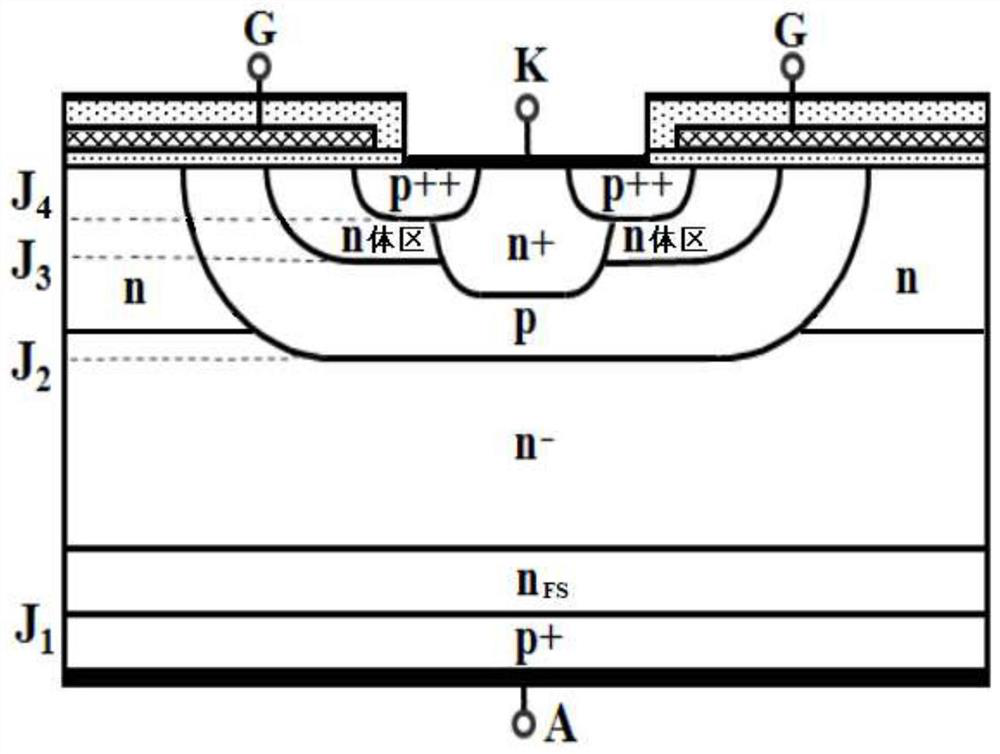
[0027] refer to figure 1 , the basic structure of the MOS control thyristor of the present invention is that the whole device is n - The drift region acts as a voltage-resistant layer, n - There is a p base area in the center above the drift region, and n areas are located on both sides of the p base area; an n area is set in the center above the p base area. + Cathode area, n + There are n body regions on both sides of the cathode region, and the n body regions on both sides and n + A p ++ source region; two p ++ The aluminum layer on the upper surface of the source region and the n + The aluminum layer on the upper surface of the cathode region is connected as a whole to form the cathode electrode K; the n region, p base region, n body region and part of the p region on both sides ++ A layer of gate oxide layer (i.e. SiO 2 Material ...


PUM


Abstract

The invention discloses a manufacturing method of an MOS control thyristor. The manufacturing method comprises the following steps: 1) forming an n drift region on the epitaxy of a substrate; 2) forming an n region in the active region; 3) forming a gate oxide layer; 4) depositing a polycrystalline silicon layer and carrying out phosphorus doping; 5) forming a p base region and a terminal p-type field limiting ring; 6) forming an n+ cathode region; 7) forming an n body region and a terminal n-type cut-off ring; 8) forming a p++ source region; 9) flattening the surface; 10) forming a metalizedcathode and a metalized grid electrode; 11) removing the substrate, and taking a transition region formed by convective diffusion between the substrate and the ndrift region as an nFS layer; 12) forming a p+ anode region; 13) forming a multi-layer metallized anode A; 14) forming a cathode and gate pressure welding area isolation pattern and a terminal passivation film; and 15) completing surface protection of the terminal region. The MOS control thyristor manufactured by adopting the method provided by the invention can meet the requirements of the fields of pulse power and solid-state circuitbreakers.

Description

technical field [0001] The invention belongs to the technical field of power semiconductor devices, and relates to a manufacturing method of a MOS control thyristor. Background technique [0002] MOS-controlled thyristors (MCTs) are simpler to drive than ordinary thyristors controlled by current because they are controlled by voltage signals. Although the traditional MCT can reduce the on-state voltage drop of the device, due to the small concentration difference between the p-base region and the n-body region, it is difficult to control the channel concentration and length during manufacturing, which not only leads to channel punch-through when the device is blocked , and the threshold voltage is very sensitive to the change of the channel, which makes the current rise rate low and the on-state voltage drop high during turn-on, thus limiting the wide application of MCT in the fields of pulse power and solid-state circuit breakers. Contents of the invention [0003] The p...

Claims


Application Information

Patent Timeline
IPC IPC(8): H01L21/332H01L29/74H01L29/06
CPCH01L29/66363H01L29/74H01L29/0603H01L29/0684
Inventor 王彩琳苏乐杨武华杨晶
Owner XIAN UNIV OF TECH
Why Eureka
Try Eureka