
A boron diffusion method for high-voltage thyristor chips

A high-voltage thyristor and diffusion method technology, applied in the field of boron diffusion, can solve problems such as reducing production efficiency, and achieve the effects of improving energy conversion efficiency, enhancing conductance modulation effect, and reducing on-state voltage drop

Active Publication Date: 2017-04-12
NINGBO SILCR POWER SEMICON
View PDF4 Cites 0 Cited by
  • Summary
  • Abstract
  • Description
  • Claims
  • Application Information

AI Technical Summary

Problems solved by technology

In order to reduce the mutual interference between adjacent high-voltage thyristor chips during boron diffusion, it is necessary to appropriately increase the spacing between each high-voltage thyristor chip during diffusion (for example: for a 3-inch chip, at least the distance between each high-voltage thyristor chip Interference can be basically eliminated by increasing the spacing to 3mm), which will reduce the number of chips per diffusion and reduce production efficiency

Method used


Image

  • A boron diffusion method for high-voltage thyristor chips
  • A boron diffusion method for high-voltage thyristor chips
  • A boron diffusion method for high-voltage thyristor chips

Examples


Embodiment Construction

[0014] The present invention will be further described in detail below in conjunction with the accompanying drawings and embodiments.

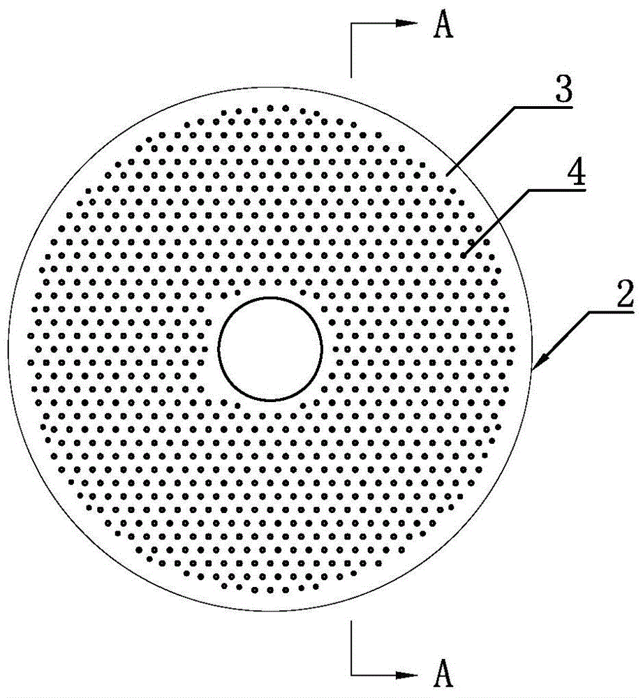
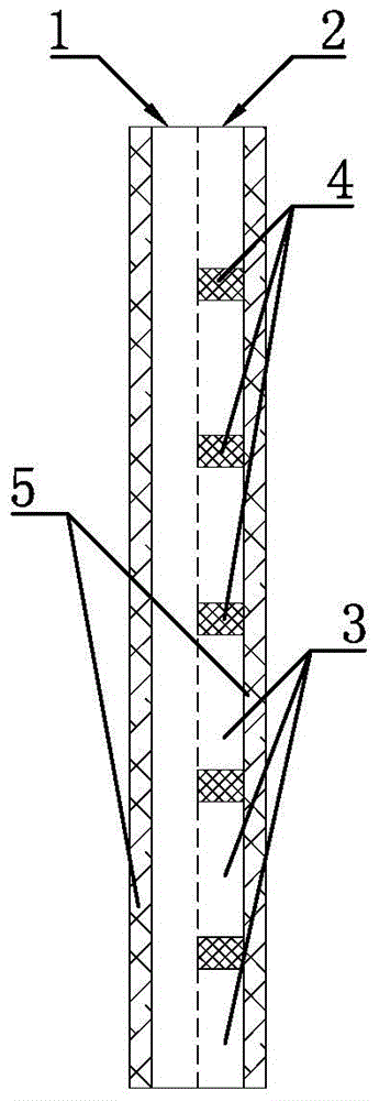
[0015] Such as Figure 1~5 As shown, the thyristor chip is divided into an anode surface and a cathode surface. Generally, the anode surface is composed of an anode (P type) 1, and the cathode surface is composed of a cathode 2 (N+ type), a gate (P type) and a short circuit point 4 (P type). , wherein the short-circuit points 4 are uniformly distributed on the cathode surface, the cathode (N+ type) 2, that is, the cathode 2 is located on the N+ phosphorus diffusion region 3, and the anode (P type) 1, that is, the anode 1 is located on the P. A method for boron diffusion of high-voltage thyristor chips, comprising the following steps: ① placing a plurality of high-voltage thyristor chips in an oxidation furnace (not shown in the figure) equidistantly with a pitch of 3 mm, and oxidizing at 1250° C. for 5 hours to make each A layer of oxide laye...


PUM

PropertyMeasurementUnit
thicknessaaaaaaaaaa

Abstract

The invention discloses a boron diffusion method of high-voltage thyristor chips. The method comprises the following steps that (1) multiple high-voltage thyristor chips are equidistantly arranged in an oxidation furnace with a spacing distance of 2-3mm, and an oxidation layer of which thickness is greater than 1.5 microns is respectively generated on the anode surface and the cathode surface of each chip after 2-10 hours of oxidation under 1200-1300 DEG C and then taken out; (2) photo-etching is performed on each chip so as to remove the oxidation layer of the anode surface of the chip and the oxidation layer of the surface of a short circuit point and retain the oxidation layer of the surface of an N+ phosphorus diffusion region phosphorus diffusion layer; (3) and the chips processed after the step (2) are equidistantly arranged in a boron diffusion furnace with the spacing distance of 0.5-1mm, a boron source of which thickness is 0.8-1.5 microns is coated on the anode surface of each chip, and boron diffusion is performed for 1-4 hours under 1200-1300 DEG C and then the chips are taken out. Voltage drop is reduced, opening speed is enhanced, current rise rate and voltage build-up rate are enhanced, leak current is reduced and the number of chips of single diffusion is increased.

Description

technical field [0001] The invention relates to a boron diffusion method, in particular to a boron diffusion method for a high-voltage thyristor chip. Background technique [0002] At present, thyristor chips are developing towards higher voltage, higher current and ultra-high control power, which inevitably requires thyristor chips to have thicker thickness, higher resistivity and larger diameter. However, the thickness of the thyristor chip and the increase in resistivity will cause the thyristor chip to produce a larger on-state voltage drop (V TM ), that is, the energy loss of the thyristor chip due to its own heating during operation is greater; at the same time, the turn-on speed of the thyristor chip will decrease, that is, the turn-on energy loss will increase, and the current rise rate (di / dt) of the thyristor chip will also increase. reduce. The thyristor chip is divided into an anode surface and a cathode surface. Generally, the anode surface is composed of an a...

Claims


Application Information

Patent Timeline
Patent Type & Authority Patents(China)
IPC IPC(8): H01L21/225H01L21/332
CPCH01L21/225H01L29/66363
Inventor 王大江王森彪徐艳艳李建忠
Owner NINGBO SILCR POWER SEMICON
Learn More