Insulated gate bipolar transistor and manufacturing method thereof

A bipolar transistor and insulated gate technology, applied in semiconductor/solid-state device manufacturing, semiconductor devices, electrical components, etc., can solve problems such as low current-carrying density, low MOSFET driving power, and large conduction voltage drop

Inactive Publication Date: 2010-11-03
商海涵
View PDF2 Cites 2 Cited by
  • Summary
  • Abstract
  • Description
  • Claims
  • Application Information

AI Technical Summary

Problems solved by technology

The driving power of MOSFET is small, the switching speed is fast, but the conduction voltage drop is large, and the current carrying density is small

Method used


Image

  • Insulated gate bipolar transistor and manufacturing method thereof
  • Insulated gate bipolar transistor and manufacturing method thereof
  • Insulated gate bipolar transistor and manufacturing method thereof

Examples


Embodiment Construction

[0017] The present invention will be described in further detail below in conjunction with the accompanying drawings and specific embodiments:

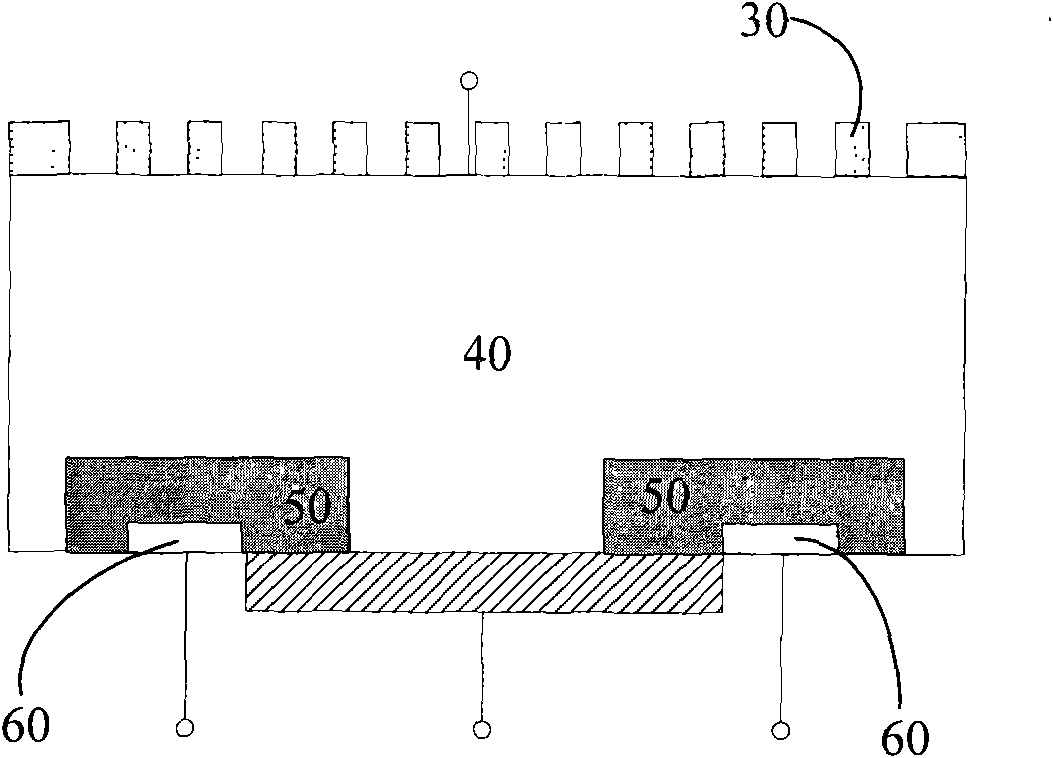
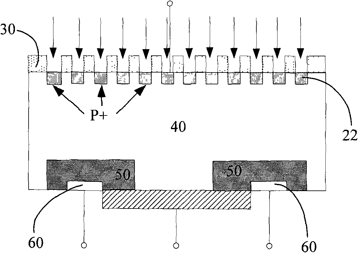
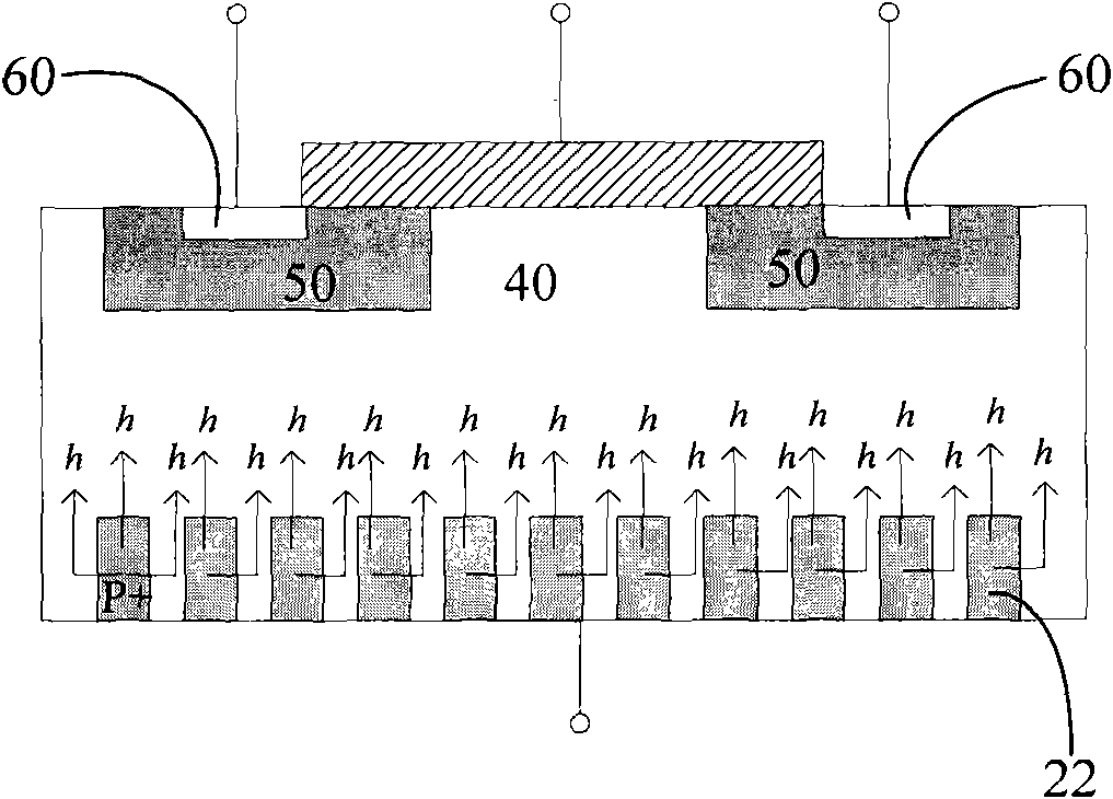
[0018] figure 1 In the first step of the method for manufacturing an insulated gate bipolar transistor of the present invention, a base material 40 is provided and a high concentration P region 50 and an N+ region 60 are formed on the front surface of the base material 40, and the back surface of the base material 40 is thinned by photolithography. The process defines the size of the backside emitter and impurity regions of the substrate. A gate is drawn out from the base material 40 , an emitter junction is drawn out from the N+ region 60 , and a collector junction is drawn out from the emitter. The photolithography process utilizes the photochemical reaction of the photosensitive resist coating 30 (photoresist), and combines the etching method to copy the mask pattern onto the photoresist. In this embodiment, the substrate is a lo...


PUM


Abstract

The invention provides an insulated gate bipolar transistor, which is manufactured by using a silicon chip. The insulated gate bipolar transistor comprises a P+ region, an N- region, a P region and an N+ region, wherein the P region and the N+ region are positioned on the front surface of the silicon chip; the P+ region is positioned on the back surface of the silicon chip; and the P+ region comprises a plurality of P-type impurity regions which are longitudinally distributed in a doping way. The invention also provides a method for manufacturing the insulated gate bipolar transistor. As the P+ region comprises the plurality of P-type impurity regions to increase the effective area of an emitter and increase injected P-type impurities, cavity minority carriers injected into the N- region are increased, conductivity modulation effect on the N- region is enhanced, the on-state voltage drop of the insulated gate bipolar transistor is reduced and the loss of own power of the insulated gate bipolar transistor is further reduced.

Description

technical field [0001] The invention relates to the field of semiconductor power device manufacturing, in particular to an insulated gate bipolar transistor (Insulated Gate Biplar Transistor, IGBT) and a manufacturing method thereof. Background technique [0002] Insulated Gate Bipolar Transistor (IGBT) is a voltage-driven power electronic device that combines the advantages of BJT (Bipolar Transistor) and MOSFET (Insulated Gate Field Effect Transistor), and has the high input of MOSFET. Both the impedance and the low on-state voltage drop of the BJT. The saturation voltage of BJT is reduced, the current carrying density is large, but the driving current is large. MOSFET drive power is small, switching speed is fast, but the on-state voltage drop is large, and the current carrying density is small. The IGBT combines the advantages of the above two devices, and the driving power is small and the saturation voltage is reduced. It is very suitable for high-voltage converter ...

Claims


Application Information

Patent Timeline
Patent Type & Authority Applications(China)
IPC IPC(8): H01L29/739H01L29/06H01L21/331H01L21/265
Inventor 商海涵
Owner 商海涵
Why Eureka
Try Eureka