High-performance super-junction structure IGBT structure and method thereof

A high-performance, p-type technology, used in electrical components, circuits, semiconductor devices, etc., can solve problems such as increasing manufacturing difficulty and cost, increasing device turn-off loss, and long device turn-off time, reducing on-resistance and The effect of forward voltage drop, reduced power consumption, and small turn-on voltage drop

Active Publication Date: 2020-09-04
苏州创芯致尚微电子有限公司
View PDF6 Cites 2 Cited by
  • Summary
  • Abstract
  • Description
  • Claims
  • Application Information

AI Technical Summary

Problems solved by technology

From the perspective of power consumption, the main problem faced by IGBT: in order to reduce the power consumption of the device, the on-resistance must be reduced first, which requires that the drift layer of the device has a higher concentration of free carriers in the on-state, however, a large number of The free carriers in the device will lead to a longer turn-off time of the device and increase the turn-off loss of the device, so there is a contradiction between reducing the on-resistance and reducing the turn-off loss, which is the main problem of IGBT
However, doping will destroy the charge balance, and irradiation has a greater impact on the service life of the device
Therefore, it was proposed to use Schottky contacts in super-junction MOSFETs to improve switching characteristics, and the third-generation COOLMOSTMC3 series improved its reverse recovery characteristics by integrating a SiC diode inside, which achieved better results but increased manufacturing costs. difficulty and cost

Method used


Image

  • High-performance super-junction structure IGBT structure and method thereof
  • High-performance super-junction structure IGBT structure and method thereof
  • High-performance super-junction structure IGBT structure and method thereof

Examples


Embodiment Construction

[0031] The following will clearly and completely describe the technical solutions in the embodiments of the present invention with reference to the accompanying drawings in the embodiments of the present invention. Obviously, the described embodiments are only some, not all, embodiments of the present invention.

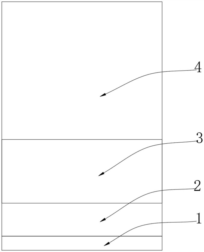
[0032] Refer to attached Figure 1-10 As shown, a p-type buffer 2 is arranged above the collector 11, an n-type buffer 3 is arranged above the p-type buffer 2, and an n+ type drift region is arranged above the n-type buffer 3 4. The inside of the n+ type drift region 4 is provided with a p-type block 5, the p-type block 5 is arranged on both sides of the interior of the n+ type drift region 4, and the top of the n+ type drift region 4 is provided with a second An etching trench 12, the bottom of the first etching trench 12 is provided with a second etching trench 13, the inside of the second etching trench 13 is provided with a p-type drain mesh block 6, and the firs...


PUM


Abstract

The invention provides a high-performance super-junction structure IGBT structure and a method thereof. The structure comprises a collector; a p-type buffer region arranged over the collector; an n-type buffer region arranged over the p-type buffer region; an n + type drift region arranged over the n type buffer region; a p-type block arranged in the n +-type drift region; a first etching groove formed in the top of the n + type drift region; a second etching groove formed in the bottom of the first etching groove; a p-type drain grid block arranged in the second etching groove; a p-type region arranged in the first etching groove; and a third etching groove formed in the top of the p-type region. The p-type block and the p-type drain grid block are arranged in a drift region, so that thedrift region is divided into three parts, the p-type block and the p-type drain grid block both play a role in blocking holes, the conductivity modulation effect is enhanced, the device has small conduction voltage drop under heavy current, the doping concentration of the drift region can be improved while the same withstand voltage is ensured, the conduction resistance and the forward voltage drop are reduced, and the power consumption is reduced.

Description

technical field [0001] The invention relates to the technical field of IGBTs, in particular to a structure of a high-performance super junction structure IGBT. Background technique [0002] At present, my country's new power electronic devices mainly include VDMOS and IGBT devices. IGBT has MOS input and bipolar output functions. It has the advantages of fast speed, high input impedance and good thermal stability. Since its inception, it has quickly developed into a mainstream power switching device in the field of medium and high power power electronics. Has been widely used in industrial control, automotive electronics, home appliances, network communications and other fields. Like other power devices, the optimization of IGBT structure mainly revolves around reducing power consumption and improving breakdown voltage. From the perspective of power consumption, the main problem faced by IGBT: in order to reduce the power consumption of the device, the on-resistance must b...

Claims


Application Information

Patent Timeline
Patent Type & Authority Applications(China)
IPC IPC(8): H01L29/06H01L21/335H01L29/778
CPCH01L29/0634H01L29/0684H01L29/66431H01L29/778
Inventor 潘庆波王新强李娜王丕龙杨玉珍
Owner 苏州创芯致尚微电子有限公司
Why Eureka
Try Eureka