Semiconductor device and manufacture method thereof

A manufacturing method and semiconductor technology, applied in semiconductor/solid-state device manufacturing, semiconductor devices, electrical components, etc., can solve the problem of poor reverse breakdown characteristics of devices, affect device electrical parameters and reliability, and cannot form Schottky potential To improve the reverse breakdown characteristics, save the area of ​​a single cell, and achieve miniaturization

Inactive Publication Date: 2012-10-17
ZHEJIANG UNIV
View PDF4 Cites 2 Cited by
  • Summary
  • Abstract
  • Description
  • Claims
  • Application Information

AI Technical Summary

Problems solved by technology

However, when this structure is reverse biased, although the inner wall of the trench uses a high barrier Schottky junction, the electric field strength in the semiconductor body at the corner of the bottom edge of the trench is easily affected by the shape of the trench and is too large, resulting in a reverse reaction of the device. At the same time, in the Schottky junction formation process, the deposited barrier metal is easy to form a void at the corner of the bottom of the trench, so the Schottky barrier junction cannot be formed here, thus affecting Device electrical parameters and reliability

Method used


Image

  • Semiconductor device and manufacture method thereof
  • Semiconductor device and manufacture method thereof
  • Semiconductor device and manufacture method thereof

Examples


Embodiment Construction

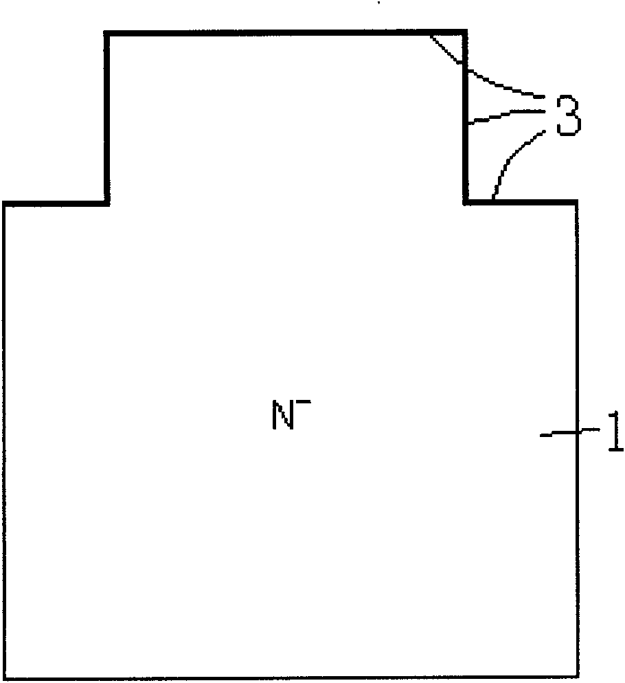
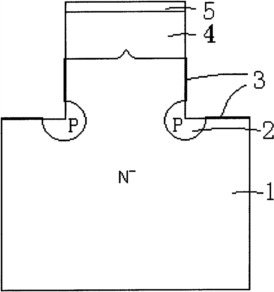
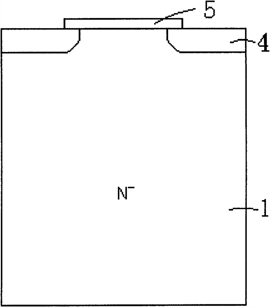
[0026] figure 2 It is a schematic cross-sectional view of a single cell of the semiconductor device of the present invention, which includes: N-type conductive semiconductor material 1, which is a lightly doped N-conductive type silicon semiconductor material, and a P-type conductive material area on the upper surface of the N-type conductive semiconductor material 4. At the same time, the depth of the trench formed by the etching process is greater than the depth of the P-type conductive material region 4; the P-type conductive material region 2 at the bottom of the trench is located in the semiconductor material body at the corner of the bottom edge of the trench; on the sidewall of the trench The surface of the N-type conductive semiconductor material and the bottom is the Schottky barrier junction 3; the oxide layer 5 is located on the surface of the semiconductor material between the trenches.

[0027] The manufacturing process includes the following steps: in the first step...


PUM


Abstract

The invention discloses a semiconductor device having a trench structure. A surface of an N-type conductive semiconductor material is provided with trenches, an entire area of an upper part of the semiconductor material between the trenches is a P-type conductive material area, and a passivation layer is disposed on an upper surface of the P-type conductive material area. The P-type conductive material area is also disposed in the semiconductor material on corners of trench bottom edges. And Schottky barrier junctions are disposed on side walls of the trenches and surfaces of a bottom N-type conductive semiconductor material. The invention also provides a manufacture method for the semiconductor device, and through the manufacture method, a rapid-recovery diode can be made by twice photolithography technique.

Description

Technical field [0001] The invention relates to a semiconductor power device, in particular to a semiconductor device with a trench structure; the invention also relates to a manufacturing method of a semiconductor device. Background technique [0002] Power semiconductor devices are widely used in power management and power applications. Especially semiconductor devices involving trench structures have become an important trend in device development. Schottky devices have the advantages of low forward turn-on voltage and fast turn-on and turn-off speed. At the same time, Schottky devices also have the disadvantages of large reverse leakage current and cannot be used in high-voltage environments. [0003] BJ Baliga, the inventor of junction barrier Schottky, proposed a trench structure Schottky device in 1993, Trench Schottky Barrier Schottky (L.Tu and BJBaliga, USPatent#5,262,668, Issued November 16, 1993.) ,Such as figure 1 As shown, the surface of the device is a trench structu...

Claims


Application Information

Patent Timeline
Patent Type & Authority Applications(China)
IPC IPC(8): H01L29/06H01L29/872H01L21/329
Inventor 丁扣宝朱江
Owner ZHEJIANG UNIV
Why Eureka
Try Eureka