A package structure of pulse power switch circuit
A pulsed power switch, circuit packaging technology, applied in circuits, pulse technology, electronic switches, etc., can solve the problems of complex circuit analysis and calculation, large influence of parasitic parameters, large stray parameters, etc., to reduce uneven current distribution, The distribution optimization of stray parameters, the effect of compact package structure
- Summary
- Abstract
- Description
- Claims
- Application Information
AI Technical Summary
Problems solved by technology
Method used
Image
Examples
Embodiment 1
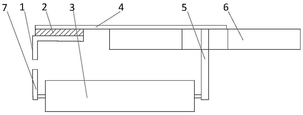
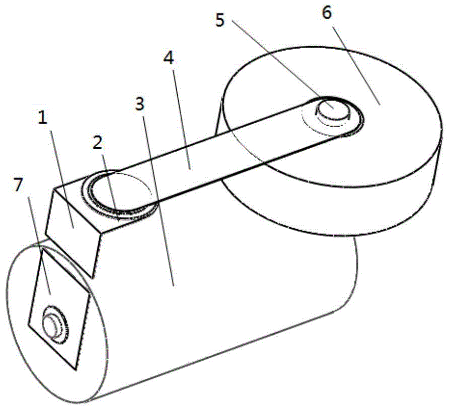
[0023] Such as figure 1 and figure 2 As shown, the packaging structure of the pulse power switch circuit includes: a first copper foil 1 , a semiconductor pulse power switch chip 2 , a capacitor 3 , a second copper foil 4 , a copper column 5 , a magnetic switch 6 and a third copper foil 7 . The magnetic switch 6 is a ring structure. One end of the capacitor 3 is welded to the third copper foil 7, and the other end is welded to one end of the copper column 5, the copper column 5 is perpendicular to the central axis of the capacitor 3, and the other end of the copper column 5 passes through the center of the magnetic switch 6 and is welded to the second copper foil 4, the second copper foil 4 is parallel to the central axis of the capacitor 3, and the other end is welded to the anode of the semiconductor pulse power switch chip 2 near the side of the capacitor 3, and the cathode of the semiconductor pulse power switch chip 2 is welded to the first copper foil 1 One end, the o...
Embodiment 2
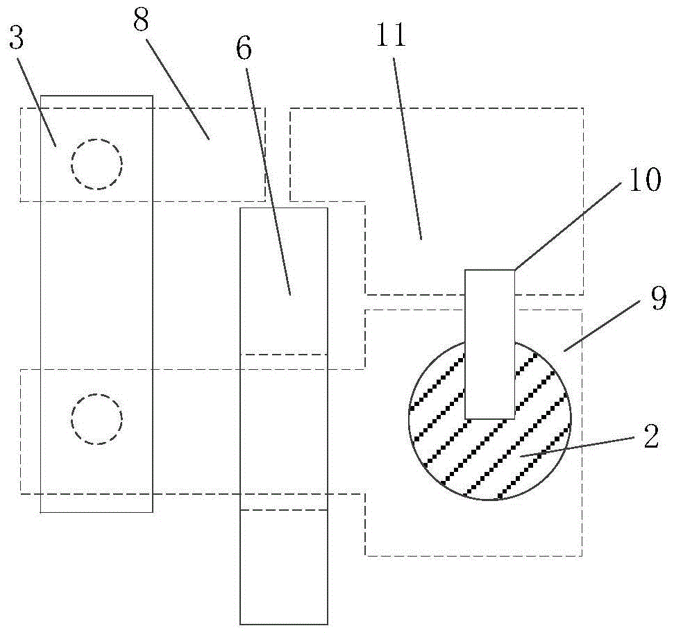
[0025] Such as image 3 and Figure 4 As shown, the package structure of pulse power switch circuit includes: semiconductor pulse power switch chip 2, capacitor 3, magnetic switch 6, first DBC copper layer block 8, second DBC copper layer block 9, copper foil 10 and third DBC copper layer Block 11. A direct bonding copper (Direct Bonding Copper, DBC) layer is designed in advance to obtain a first DBC copper layer block 8 , a second DBC copper layer block 9 and a third DBC copper layer block 11 . The magnetic switch 6 is a ring structure, the second DBC copper layer block 9 passes through the center of the magnetic switch 6, and the two ends of the capacitor 3 are respectively welded on the first DBC copper layer block 8 and the second DBC copper layer block 9, and the semiconductor pulse The anode of the power switch chip 2 is welded on the second DBC copper layer block 9 , and the cathode is welded on the third DBC copper layer block 11 through the copper foil 10 . The mag...
PUM
 Abstract
Description
Claims
Application Information


