light emitting device

A light-emitting device and packaging layer technology, which is applied in the direction of semiconductor devices, electrical components, circuits, etc., can solve the problems of large package structure, increased package thickness, and high cost of quartz glass, so as to reduce costs, improve transmittance, and product size. The effect of shrinking

Active Publication Date: 2022-05-10
QUANZHOU SANAN SEMICON TECH CO LTD
View PDF9 Cites 0 Cited by
  • Summary
  • Abstract
  • Description
  • Claims
  • Application Information

AI Technical Summary

Problems solved by technology

However, due to the cavity and the certain thickness of the ceramic bowl, the package structure is too large, and there is no way to adjust the light angle and spatial distribution of light intensity of the package.
[0003] In order to change the light-emitting angle, a quartz glass lens is usually added on the light-emitting surface, which further increases the thickness of the package, and the cost of quartz glass is high

Method used


Image

  • light emitting device
  • light emitting device
  • light emitting device

Examples


Embodiment 1

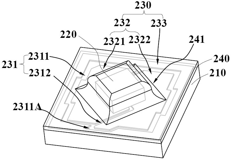
[0038] Please see attached. Figure 2 This embodiment discloses an ultraviolet packaging device, which comprises a packaging substrate 210, a patterned conductive layer 230 on the upper surface of the substrate, an LED chip 220 arranged on the substrate 210 and electrically connected with the conductive layer 230, and a packaging layer 240 covering the upper surface of the substrate and the LED chip 220. The packaging layer 240 forms an optical structure at the corresponding position of the LED chip 220, and the optical structure is above and / or above the LED chip.

[0039] Specifically, the substrate 210 includes an upper surface and a lower surface, and the substrate 210 can be made of materials commonly used in the art, such as ceramic or silicon, preferably a ceramic substrate. The size of the substrate can be selected according to requirements, such as 3535 or 2319 or 1313.

[0040] The conductive layer 230 is formed on the upper surface of the substrate 210, patterned, and di...

Embodiment 2

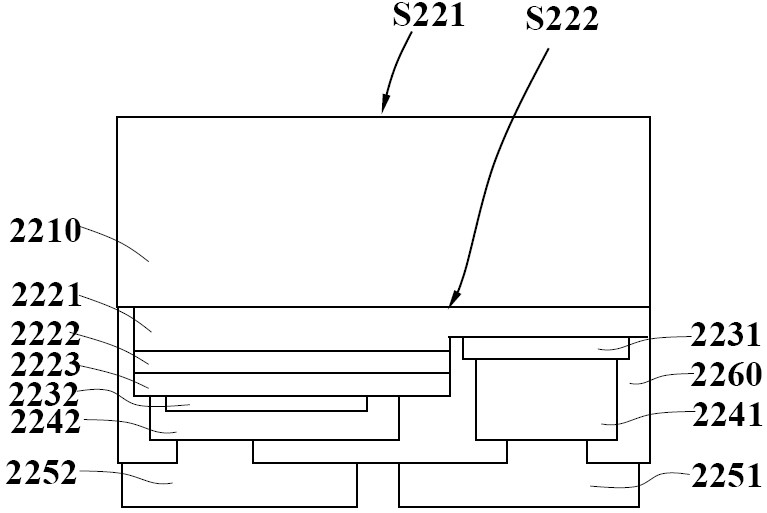
[0054] Figure 7 A light emitting device implemented according to the present invention is shown. at Figure 4 In the illustrated light emitting device, the thickness of the LED chip is more than 300μm, and the thickness t of the encapsulation layer 240 30 Less than the thickness of the LED chip. In the light emitting device shown in this embodiment, the thickness t of the LED chip 20 300μm or less, for example, 150μm to 200μm, or 200μm to 300μm, the first thickness T of the encapsulation layer 240 31 And the thickness t of the LED chip 220 20 The relationship is preferably 1.2T 20 ≥T 31 ≥0.5T 20 At this time, the packaging layer 240 can better cover the LED chip 240, and an optical structure with a curved surface, such as T, is formed above the LED chip. 31 ≈T 20 . Furthermore, 0μm≤T 31 -T 32 ≤50μm, that is, the thickness of the encapsulation layer 240 on the upper surface of the LED chip is relatively uniform. Furthermore, the thickness of the packaging layer 240 in each area is ...

Embodiment 3

[0058] Figure 8 A light emitting device implemented according to the present invention is shown. In this embodiment, based on the first embodiment, a series of additional grooves 2313 are formed in the edge region 233 of the patterned conductive layer 230 on the substrate, and the depth of the additional grooves 2313 is preferably more than half the thickness of the patterned conductive layer, or it can be greater than or equal to the thickness of the conductive layer 230. The encapsulation layer 240 fills the additional grooves 2313, thus increasing the bonding force between the encapsulation layer 240 and the substrate 210.


PUM

PropertyMeasurementUnit
thicknessaaaaaaaaaa
thicknessaaaaaaaaaa
thicknessaaaaaaaaaa

Abstract

The invention discloses a light-emitting device, comprising: a package substrate having opposite first and second surfaces, a patterned conductive layer is arranged on the first surface, and the patterned conductive layer is at least divided into two parts by a spacer. Two first and second regions electrically isolated from each other; the LED chip is mounted on the patterned conductive layer and has opposite upper surfaces, lower surfaces, and side walls, and the lower surface is provided with a first electrode and a second electrode. Two electrodes, wherein the first electrode is electrically connected to the first region, and the second electrode is electrically connected to the second region; an encapsulation layer covering the first surface of the LED chip and the substrate, the encapsulation layer on the A curved surface is formed at the corresponding position of the LED chip, and the part of the encapsulation layer covering the patterned conductive layer has a plane, and the distance D between the junction of the curved surface and the plane to the side wall of the LED chip is the thickness of the chip between 1 and 2 times.

Description

Technical field [0001] The invention relates to the technical field of LED packaging, in particular to a light emitting device. technical background [0002] The existing conventional deep ultraviolet LED packaging structure mainly adopts a ceramic bowl as a bearing substrate and a Shi Ying glass packaging cover. Specifically, the ultraviolet LED chip 120 with a flip-chip structure is fixed in the bowl of the packaging substrate 110 by solder paste or eutectic welding, and the chip electrode of the ultraviolet LED chip 120 is bonded with the substrate electrode 130 in the bowl, and then a Shi Ying glass plate 140 is fixed at the opening of the bowl to form a closed chamber in the bowl, such as Figure 1 Shown. However, due to the cavity and the thickness of the ceramic bowl, the package structure is too large, and there is no way to adjust the luminous angle and light intensity spatial distribution of the package. [0003] In order to change the light emitting angle, a Shi Ying gl...

Claims


Application Information

Patent Timeline
Patent Type & Authority Patents(China)
IPC IPC(8): H01L33/54H01L33/56H01L33/58H01L33/48H01L33/62
CPCH01L33/54H01L33/56H01L33/58H01L33/48H01L33/62
Inventor 黄森鹏刘健林秋霞余长治徐宸科
Owner QUANZHOU SANAN SEMICON TECH CO LTD
Why Eureka
Try Eureka