Semiconductor assembly and manufacturing method thereof
一种制造方法、半导体的技术,应用在半导体/固态器件制造、半导体器件、半导体/固态器件零部件等方向,能够解决电气短路、焊盘破裂、变形等问题,达到缩小间距的效果
- Summary
- Abstract
- Description
- Claims
- Application Information
AI Technical Summary
Problems solved by technology
Method used
Image

Examples
Embodiment Construction
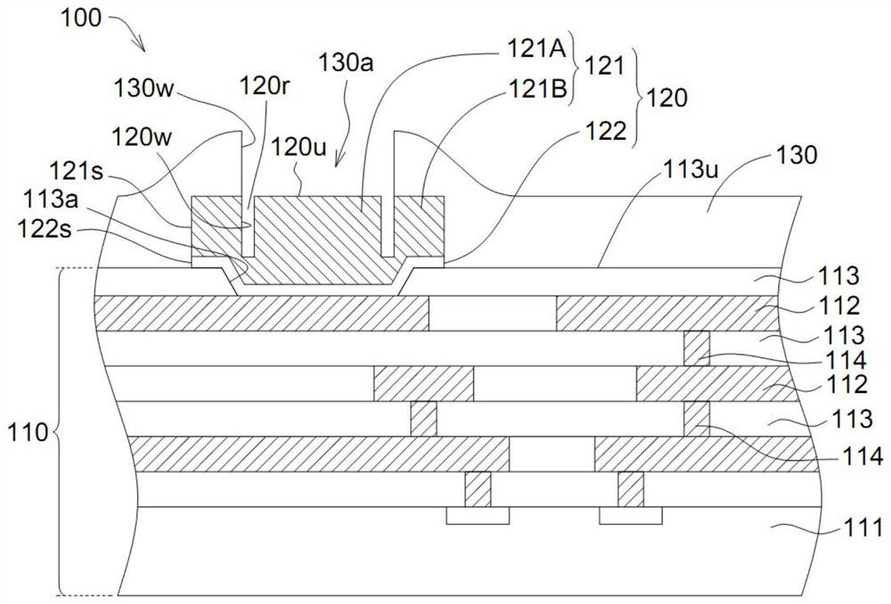
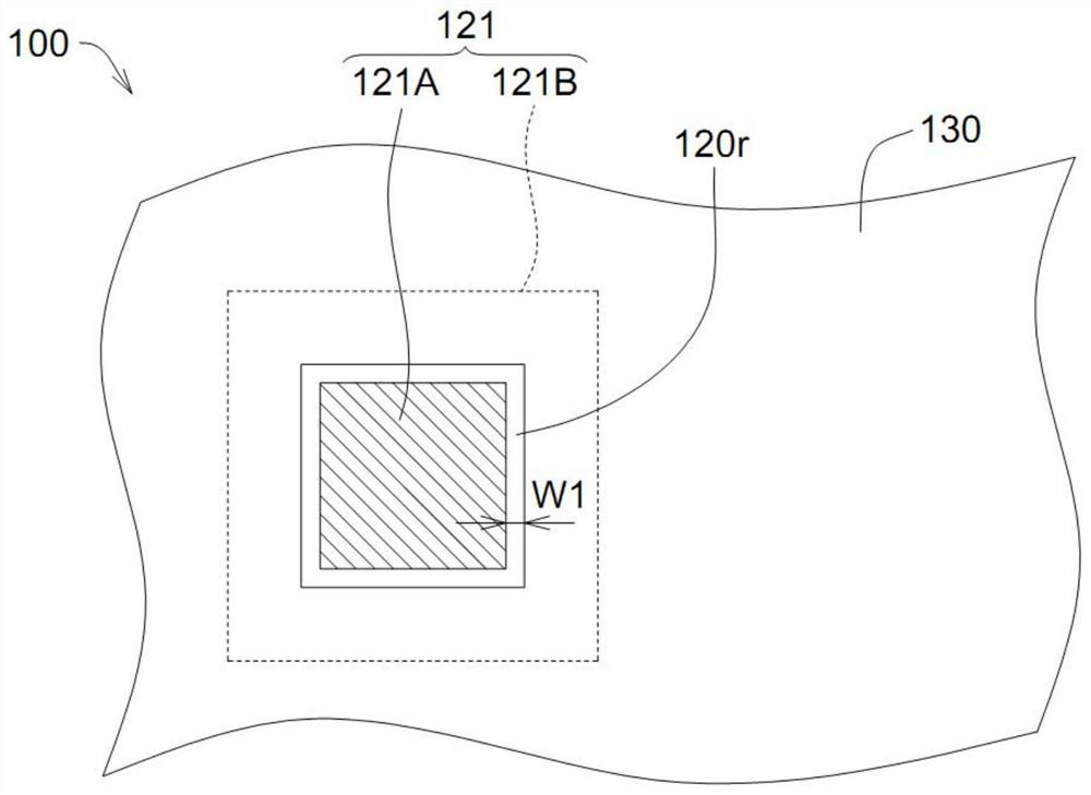
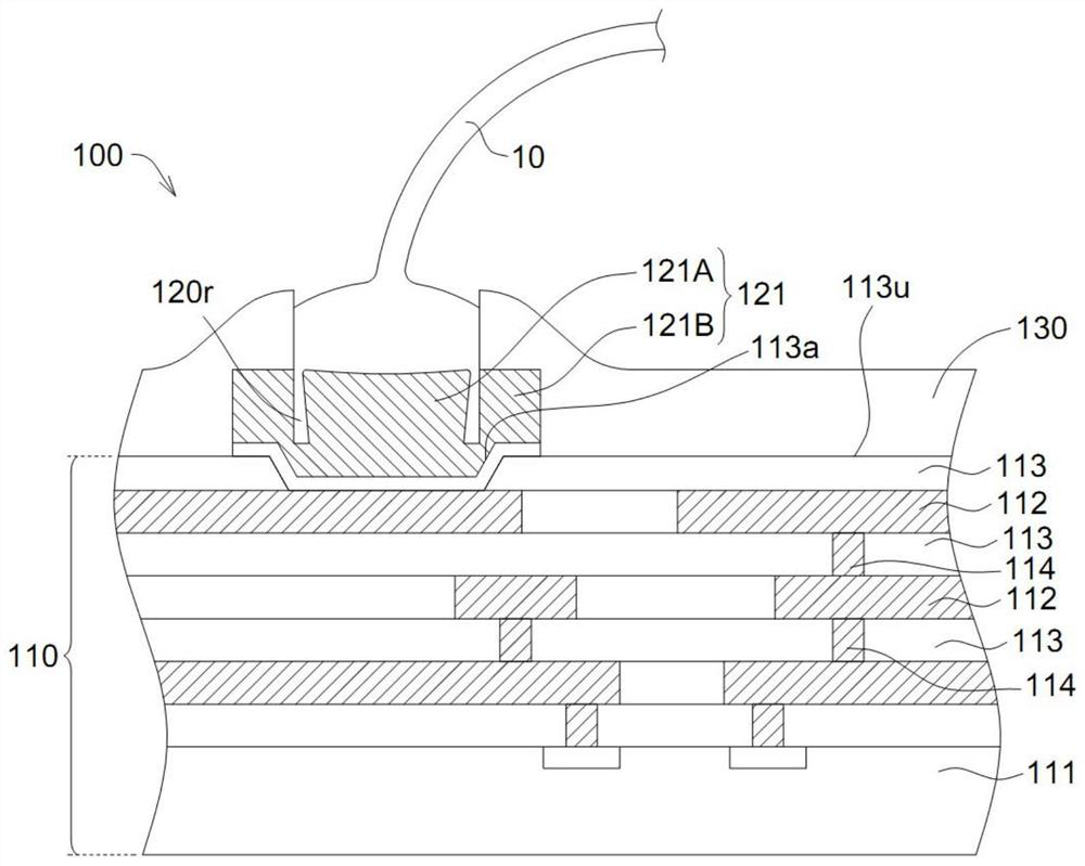
[0013] refer to Figure 1A to Figure 1C , Figure 1A shows a schematic diagram of a semiconductor assembly 100 according to an embodiment of the present invention, Figure 1B show Figure 1A A top view of the semiconductor assembly 100, Figure 1C shows the engagement in the Figure 1A A schematic diagram of bonding wires on the bonding pads 120 of the semiconductor component 100 . In one embodiment, the semiconductor component 100 may be, for example, a semiconductor substrate, a semiconductor chip, or the like.
[0014] The semiconductor assembly 100 includes a substrate 110 , at least one pad 120 and a passivation layer 130 .
[0015] The substrate 110 includes a base 111 , a plurality of conductive layers 112 , a plurality of dielectric layers 113 and a plurality of conductive vias 114 . The substrate 111 is, for example, a silicon wafer. The conductive layer 112, the dielectric layer 113, and the conductive via 114 are formed on the substrate 111 by using a semiconduc...
PUM
 Abstract
Description
Claims
Application Information
 - R&D
- Intellectual Property
- Life Sciences
- Materials
- Tech Scout
- Unparalleled Data Quality
- Higher Quality Content
- 60% Fewer Hallucinations
Browse by: Latest US Patents, China's latest patents, Technical Efficacy Thesaurus, Application Domain, Technology Topic, Popular Technical Reports.
© 2025 PatSnap. All rights reserved.Legal|Privacy policy|Modern Slavery Act Transparency Statement|Sitemap|About US| Contact US: help@patsnap.com