GaN HEMT scaling model circuit topological structure

A circuit topology and model technology, applied in the direction of electrical digital data processing, special data processing applications, instruments, etc., can solve the problems of look-up table range and huge data, discontinuous relationship, difficult to guarantee accuracy, etc., to solve model accuracy and The problem of ductility, meeting the requirements of circuit simulation, and the effect of meeting temperature change characteristics

Inactive Publication Date: 2021-02-26
TIANJIN UNIV
View PDF5 Cites 0 Cited by
  • Summary
  • Abstract
  • Description
  • Claims
  • Application Information

AI Technical Summary

Problems solved by technology

[0006] Among them, the look-up table model is based on a large amount of test data and has high precision. However, it is difficult to guarantee the accuracy of the prediction data outside the measurement range. The form of the table is used to store the input and output responses of the transistor and the parameter values ​​and external bias. Corresponding relationship of setting voltage
The advantage of the lookup table model is that it does not need to extract parameters and establish an equivalent circuit, which is intuitive and simple. However, its disa

Method used


Image

  • GaN HEMT scaling model circuit topological structure

Examples


Example Embodiment

[0025]In order to make the technical means realized by the present invention easier to understand, the application will be further described in detail below with reference to the accompanying drawings and embodiments.
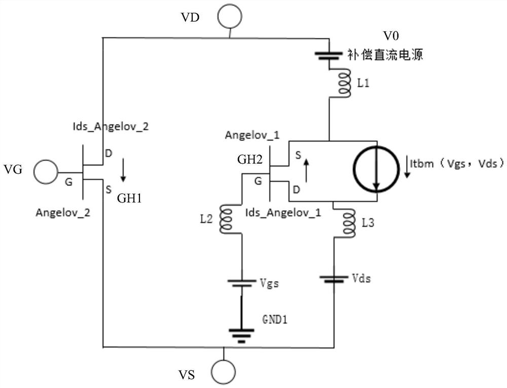
 It is understandable that the specific embodiments described here are only used to explain the related application, but not to limit the application. In addition, it should be noted that, for ease of description, only parts related to the present application are shown in the drawings.

[0026]It should be noted that the embodiments in the application and the features in the embodiments can be combined with each other if there is no conflict. Hereinafter, the present application will be described in detail with reference to the drawings and in conjunction with embodiments.

[0027]Seefigure 1The present invention provides a GaN HEMT scaling model circuit topology, which is a GaN HEMT (HEMT for high electron mobility transistor) scaling model circuit based on a lookup table mo...


PUM


Abstract

The invention discloses a GaN HEMT scaling model circuit topological structure, which is characterized in that a grid electrode G, a source electrode S and a drain electrode D of a transistor GH1 arerespectively connected with positive electrodes of direct-current power supplies VG, VS and VD; a grid electrode G, a source electrode S and a drain electrode D of the transistor GH2 are respectivelyconnected with one end of the inductor L2, one end of the inductor L1 and one end of the inductor L3; the other end of the inductor L2 is connected with the positive electrode of a direct-current power supply Vgs; the other end of the inductor L1 is connected with the negative electrode of the direct-current power supply V0; the other end of the inductor L3 is connected with the positive electrodeof a direct-current power supply Vds; wherein the source electrode S and the drain electrode D of the transistor GH2 are also connected with the two ends of the meter-based current source. Accordingto the GaN HEMT scaling model circuit topological structure disclosed by the invention, the problems of model precision and ductility can be solved, and the temperature change characteristic is met atthe same time, so that higher model precision is achieved, and the circuit simulation requirement is met.

Description

technical field [0001] The invention relates to the technical field of semiconductor device modeling, in particular to a GaN HEMT scaling model circuit topology. Background technique [0002] With the deepening of GaN (gallium nitride) research and the improvement of product technology, the reliability of GaN microwave power devices has been continuously improved, and it has moved from the laboratory to the market and is widely used in civil and national defense fields. [0003] For a fixed feature size (gate length) process, since the total output power of the transistor device is proportional to the total gate width of the device tube, in the design of microwave and millimeter-wave GaN circuits, especially the design of monolithic microwave integrated circuits, the gate of the device model Exponential and unit width scales require an optimal choice to achieve the best circuit performance. Therefore, the modeling method of large-signal scalable models is of great significa...

Claims


Application Information

Patent Timeline
IPC IPC(8): G06F30/367
CPCG06F30/367
Inventor 毕磊
Owner TIANJIN UNIV
Why Eureka
Try Eureka