

Preparation method of silicon-based OLED panel
A panel and silicon-based technology, applied in the field of silicon-based OLED panel preparation, can solve the problems of reduced service life of FMM finished products, limitation of OLED panel resolution, cost increase, etc., and achieve the effect of improving display brightness and resolution
- Summary
- Abstract
- Description
- Claims
- Application Information
AI Technical Summary
Problems solved by technology
Method used
Image


Examples
Embodiment Construction
[0029] The specific embodiment of the present invention will be described in further detail by describing the embodiments below with reference to the accompanying drawings, the purpose is to help those skilled in the art to have a more complete, accurate and in-depth understanding of the concept and technical solutions of the present invention, and contribute to its implementation.
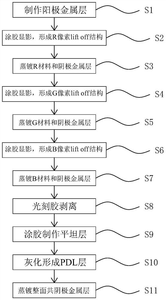
[0030] Such as figure 1 As shown, the invention provides a method for preparing a silicon-based OLED panel, comprising the steps of:
[0031] S1, making the anode metal layer;
[0032] S2. Glue-coating and developing to form an R pixel lift off structure;
[0033] S3, evaporating the R material and the cathode metal layer;
[0034] S4, glue development, forming a G pixel lift off structure;
[0035] S5, evaporating the G material and the cathode metal layer;
[0036] S6. Glue coating and development to form a B pixel lift off structure;
[0037] S7, evaporating material B and a cathode metal...
PUM
 Abstract
Description
Claims
Application Information