Deep junction composite terminal structure of high-voltage power chip and preparation method thereof

A compound terminal and power chip technology, which is applied in the direction of electrical components, circuits, semiconductor devices, etc., can solve problems such as large chip area, complex structure design of field plate plus field ring, and influence of VLD and JTE structure interface charges, etc.

Inactive Publication Date: 2021-02-26
NORTH CHINA ELECTRIC POWER UNIV (BAODING) +1
View PDF6 Cites 0 Cited by
  • Summary
  • Abstract
  • Description
  • Claims
  • Application Information

AI Technical Summary

Problems solved by technology

At present, for power semiconductor devices, the structural design of the terminal area is mainly field ring structure, field plate plus field ring composite structure, etc. However, the field ring structure occupies a large chip area and is greatly affected by interface charges, and the field plate plus field ring composite structure Complex structure design
And for high-voltage deep-junction power devices, there is still the problem of curvature concentration at the end of VLD, and the structure of VLD and JTE is greatly affected by interface charges

Method used


Image

  • Deep junction composite terminal structure of high-voltage power chip and preparation method thereof
  • Deep junction composite terminal structure of high-voltage power chip and preparation method thereof
  • Deep junction composite terminal structure of high-voltage power chip and preparation method thereof

Examples


Embodiment Construction

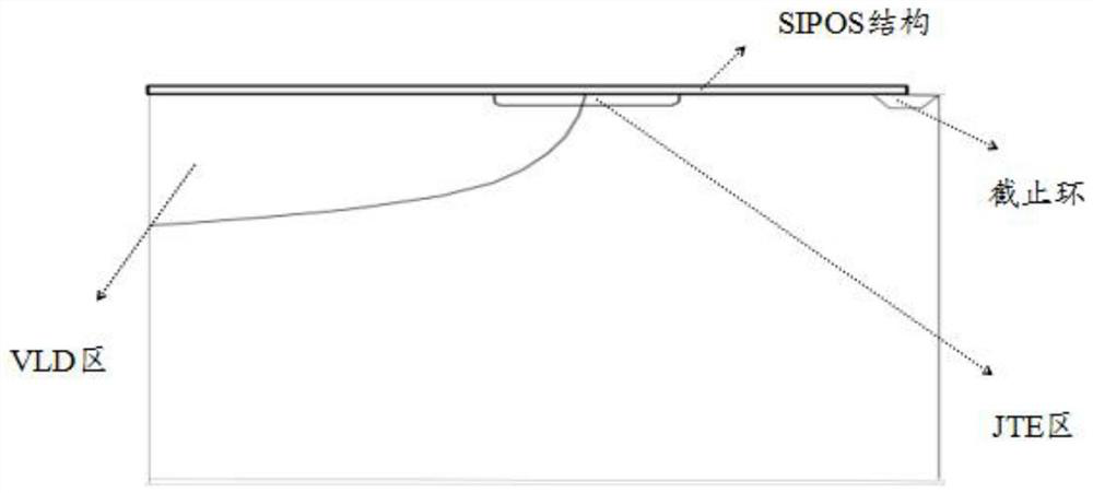
[0031] The purpose of the present invention is to provide a deep-junction composite terminal structure of a high-voltage power chip and its preparation method, so as to reduce the area of ​​the terminal area, improve its terminal efficiency, and reduce the impact of interface charges on the breakdown voltage of the terminal structure.

[0032] In order to make the above objects, features and advantages of the present invention more comprehensible, the invention will be further described in detail below in conjunction with the accompanying drawings and specific embodiments.

[0033] The insulating oxide film cannot effectively prevent the accumulation of charges on the surface of the device and ion contamination. These charges can induce charges of opposite polarity near the surface of the silicon substrate, which changes the electric field on the surface of the device, resulting in a change in the reverse breakdown voltage of the PN junction. .

[0034] The SIPOS structure has...


PUM

PropertyMeasurementUnit
Lengthaaaaaaaaaa
Thicknessaaaaaaaaaa
Resistivityaaaaaaaaaa

Abstract

The invention discloses a deep junction composite terminal structure of a high-voltage power chip. The composite terminal structure comprises a lateral variable doping region, a junction terminal extension region and an SIPOS structure; thelateral variable doping region is a region formed by injecting aluminum ions under the shielding of a plurality of different gradient doping region windows andthen performing high-temperature diffusion; the junction termination extension region is arranged at the tail end of the lateral variable doping region (VLD) and is partially overlapped with the lateral variable doping region, and the junction termination extension region (JTE) is a region formed by diffusion of boron ions at a high temperature; and the SIPOS structure is arranged at the upper parts of the transverse variable doping region and the lateral variable doping region. According to the invention, the SIPOS structure covers thelateral variable doping region and the junction terminal extension region, so that the area of the terminal region is reduced, the terminal efficiency is improved, the influence of interface charges on the breakdown voltage of the terminal structure is reduced, and the 3.3 kV-level withstand voltage requirement is met in the presence of the interface charges.

Description

technical field [0001] The invention relates to the technical field of semiconductor device design, in particular to a deep-junction compound terminal structure of a high-voltage power chip and a preparation method thereof. Background technique [0002] The design of the terminal structure is one of the key technologies of semiconductor devices, which is closely related to the breakdown voltage of the device. [0003] When the semiconductor device is reverse-biased, the pn junction inside the device extends to the surface, making the peak electric field on the surface higher than that in the body, causing breakdown to occur on the surface. At the same time, when impact ionization occurs on the surface, the heat generated by the ionization process Carriers are easy to enter the passivation layer, forming fixed charges inside the passivation layer, changing the electric field distribution, making the device performance unstable and reliability reduced. Terminal technology is ...

Claims


Application Information

Patent Timeline
IPC IPC(8): H01L29/06
CPCH01L29/0615H01L29/0684
Inventor 李学宝王振硕马慧远马浩
Owner NORTH CHINA ELECTRIC POWER UNIV (BAODING)
Why Eureka
Try Eureka