A kind of manufacturing method of igbt

A manufacturing method, N-type technology, applied in the field of IGBT manufacturing, can solve problems such as reducing the breakdown voltage of devices, and achieve the effect of strong practicability, easy use and promotion

Active Publication Date: 2021-11-26
苏州达晶微电子有限公司
View PDF3 Cites 0 Cited by
  • Summary
  • Abstract
  • Description
  • Claims
  • Application Information

AI Technical Summary

Problems solved by technology

But because the resistivity of N-type CS is lower than that of N-drift region, the introduction of CS layer will reduce the breakdown voltage of the device

Method used


Image

  • A kind of manufacturing method of igbt
  • A kind of manufacturing method of igbt
  • A kind of manufacturing method of igbt

Examples


Embodiment 1

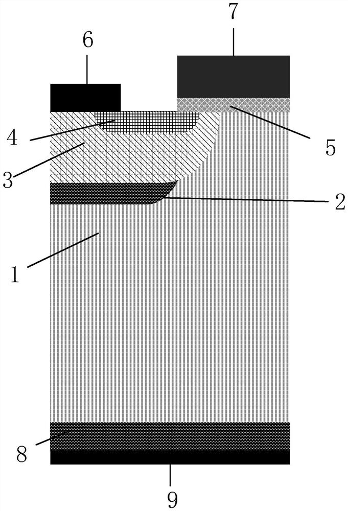
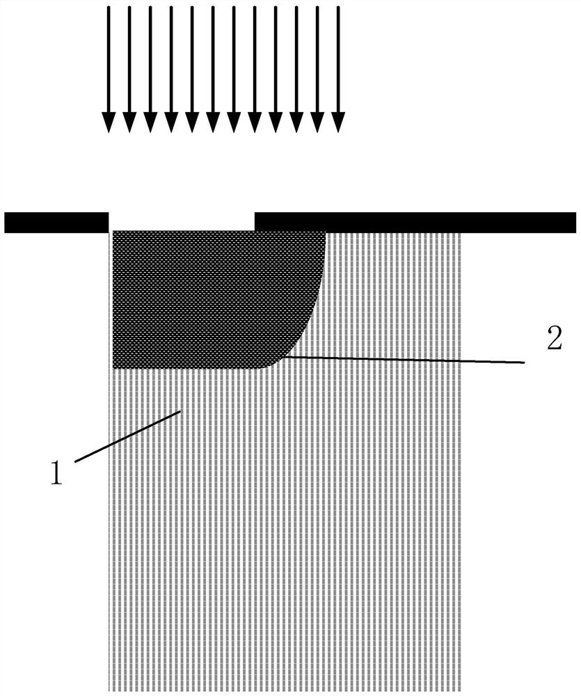
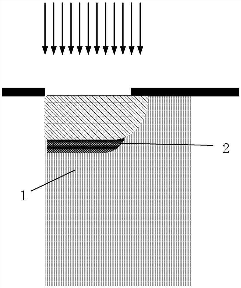
[0023] see Figure 1~3 , in an embodiment of the present invention, a method for manufacturing an IGBT includes the following steps: using an N-type single crystal silicon wafer to prepare an N-type substrate, and the N-type substrate is the N-drift region (1), and in the N-drift The upper surface of the region (1) forms an N+ minority carrier storage layer region (2), and then forms a P+ region (3) in the N+ minority carrier storage layer region (2), and the P+ region (3) completely covers the N+ minority carrier storage layer region (2) laterally. ) and does not completely cover the N+ minority carrier storage layer region (2) in the longitudinal direction, so as to achieve the purpose of only retaining the N+ minority carrier storage layer below the P+ region (3), and then normally form the front planar MOS structure, including the N+ source region (4) , gate oxide layer (5), emitter metal (6), gate metal (7) and other parts. Then, processes such as back thinning, implanta...

Embodiment 2

[0030] Taking the manufacturing process of 600V IGBT as an example, the specific process is as follows:

[0031] 1. Substrate material preparation, using an n-type zone-fused monocrystalline silicon substrate with a resistivity of about 40Ω·cm and a thickness of 400-600μm, and its crystal orientation is ;

[0032] 2. Forming an N+ doped region 2 on the N-drift region 1 by photolithography, implantation, and diffusion, and implanting a dose. Phosphorus implant dose is 1e13cm-3, implant energy is 100KeV, diffusion temperature is 1100°C, and diffusion time is 60 minutes.

[0033] 3. Form a lithography area larger than the N+ doping area. The width of the lithography opening in the P+ area is 2 μm to 6 μm larger than that in the N+ doping area. The P+ area 3 is formed in the N+ doping area 2 through the implantation and diffusion of boron. , the dose of boron implantation is 5e13cm-3, the implantation energy is 80KeV, the diffusion temperature is 1100°C, and the diffusion time is...


PUM

PropertyMeasurementUnit
electrical resistivityaaaaaaaaaa
thicknessaaaaaaaaaa

Abstract

The invention discloses a method for manufacturing an IGBT. First, an N+ minority carrier storage region is formed on an N-substrate, and then a window is formed through a photolithographic field of view larger than the N+ minority carrier storage region, so as to ensure that the P+ region can be completely Cover the N+ minority carrier storage area to form a P+ area half-surrounded by the N+ minority carrier storage layer. This method not only introduces the CS area, but also minimizes the impact of the CS layer on the breakdown voltage of the device, and finally obtains a planar localization The minority carrier storage IGBT not only effectively improves the trade-off relationship between turn-on voltage drop and turn-off loss, but also minimizes the influence of the minority carrier storage region on the breakdown voltage of the device. The invention has strong practicability and is easy to use and popularize.

Description

technical field [0001] The invention relates to semiconductor technology, in particular to a method for manufacturing an IGBT. Background technique [0002] IGBT (Insulated Gate Bipolar Transistor, Insulated Gate Bipolar Transistor) is a bipolar device. From a structural point of view, the front is a MOSFET structure, and the back is a PIN diode structure. Through the combination of this structure, so that The IGBT not only has the characteristics of a bipolar power transistor with low conduction voltage and large current capacity, but also has the advantages of a high input impedance of a power MOSFET and a simple driving circuit. With the popularization of electrification, IGBT is used more and more widely, such as: new energy vehicles, high-speed rail, industrial frequency conversion, white goods and other fields. The reason why the IGBT has a low on-state voltage drop is mainly that a large amount of excess carriers are stored in the N-drift region during the turn-on pr...

Claims


Application Information

Patent Timeline
Patent Type & Authority Patents(China)
IPC IPC(8): H01L29/739H01L29/06H01L21/331
CPCH01L29/0623H01L29/0684H01L29/66333H01L29/7396H01L29/7398
Inventor 廖兵沈礼福
Owner 苏州达晶微电子有限公司
Why Eureka
Try Eureka