Organic light-emitting display panel and manufacturing method thereof and organic light-emitting display device

A light-emitting display and organic technology, applied in the direction of organic semiconductor devices, semiconductor/solid-state device manufacturing, electrical components, etc., can solve the problems of micro-display display effects, image brightness, color gamut, power consumption degradation, etc., to avoid image brightness Uniformity degradation and color display accuracy degradation, reduction of loss of luminous flux, effects of color gamut increase

Inactive Publication Date: 2021-03-02
SEEYA OPTRONICS LTD
View PDF7 Cites 1 Cited by
  • Summary
  • Abstract
  • Description
  • Claims
  • Application Information

AI Technical Summary

Problems solved by technology

However, based on these obviously conflicting design requirements, along with the reduction in device size, if the design of medium-sized or even large-sized display screens such as mobile phones and computers is continued, the brightness, color gamut, and power consumption of the displayed image will be significantly reduced. Deterioration, affecting the display effect of the micro-display

Method used


Image

  • Organic light-emitting display panel and manufacturing method thereof and organic light-emitting display device
  • Organic light-emitting display panel and manufacturing method thereof and organic light-emitting display device
  • Organic light-emitting display panel and manufacturing method thereof and organic light-emitting display device

Examples


Embodiment Construction

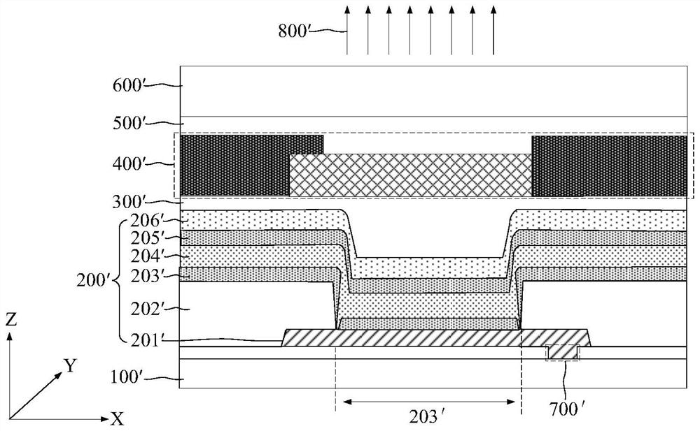
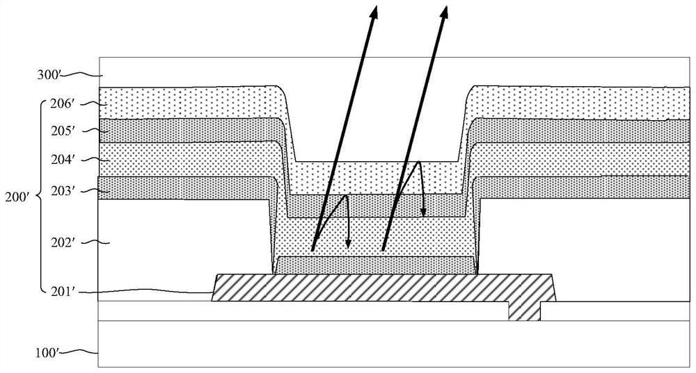
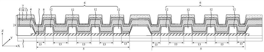
[0040] In order to make the purpose, technical solutions and advantages of the embodiments of the present invention clearer, the technical solutions in the embodiments of the present invention will be clearly and completely described below in conjunction with the drawings in the embodiments of the present invention. Obviously, the described embodiments It is a part of embodiments of the present invention, but not all embodiments. All other structures and embodiments obtained by those skilled in the art based on the embodiments and the concepts and methods disclosed in the present invention belong to the protection scope of the present invention.

[0041] Terms used in the embodiments of the present invention are only for the purpose of describing specific embodiments, and are not intended to limit the present invention. As used in the embodiments of the present invention and the appended claims, the singular forms "a", "said" and "the" are also intended to include the plural f...


PUM

PropertyMeasurementUnit
electron work functionaaaaaaaaaa
thicknessaaaaaaaaaa

Abstract

The embodiment of the invention provides an organic light-emitting display panel and a manufacturing method thereof and an organic light-emitting display device, and relates to the technical field ofdisplay. The panel comprises a light-emitting device layer arranged on a substrate, and the panel comprises: a first electrode; a pixel definition layer which is located on the side, back on to the substrate, of the first electrode, wherein the pixel definition layer is provided with a plurality of opening areas, and part of the first electrode is exposed in the opening areas; a retaining wall structure which is positioned in the opening area and is back to one side of the substrate; a light-emitting functional layer arranged at one side, back to the substrate of the pixel definition layer, the opening area and the retaining wall structure; and a second electrode which is positioned on one side, back to the substrate, of the light-emitting functional layer. The retaining wall structure comprises retaining walls, and concave areas are arranged between the retaining walls and the pixel definition layer or between the retaining walls or in the retaining walls. The film thickness of the second electrode at the top of the retaining wall is greater than that of the side wall of the retaining wall and the sunken area. According to the embodiment of the invention, the luminous flux outputby the panel is effectively improved, and meanwhile, the square resistance of the cathode film layer can be prevented from being greatly increased.

Description

【Technical field】 [0001] The present invention relates to the field of display technology, in particular to an organic light emitting display panel, a manufacturing method thereof, and an organic light emitting display device. 【Background technique】 [0002] With the development of organic light emitting diode (Organic Light Emitting Diode, OLED) display technology and the expansion of large-scale manufacturing industry, OLED display has become the mainstream of mobile display, occupying a considerable market share of medium-sized or even large-sized display screens. [0003] However, when OLED display technology gradually penetrates into some special display application fields, such as augmented reality (Augment Reality, AR) and virtual reality (Virtual Reality, VR) display fields, the constraints of the original device structure on the display performance gradually become revealed. Take the microdisplay in AR and VR glasses as an example. This type of microdisplay needs t...

Claims


Application Information

Patent Timeline
Patent Type & Authority Applications(China)
IPC IPC(8): H01L27/32H01L51/56H01L51/52
CPCH10K59/122H10K71/164H10K50/805H10K50/813H10K50/828H10K2102/3026H10K2102/351H10K50/822H10K71/00H10K71/60H10K59/1201
Inventor 黄忠守
Owner SEEYA OPTRONICS LTD
Why Eureka
Try Eureka