Spraying method of wafer-level sensitive material and semiconductor sensor

A sensitive material, wafer-level technology, applied in the field of sensors, which can solve the problems of poor performance consistency, high cost, and inability to solve high-volume manufacturing.

Inactive Publication Date: 2021-03-05
AEROSPACE INFORMATION RES INST CAS +1
View PDF9 Cites 0 Cited by
  • Summary
  • Abstract
  • Description
  • Claims
  • Application Information

AI Technical Summary

Problems solved by technology

This method not only cannot solve the problem of mass production, resulting in high cost, but also the performance consistency of each sensor prepared by this method is poor

Method used


Image

  • Spraying method of wafer-level sensitive material and semiconductor sensor
  • Spraying method of wafer-level sensitive material and semiconductor sensor
  • Spraying method of wafer-level sensitive material and semiconductor sensor

Examples


Embodiment Construction

[0020] In order to make the object, technical solution and advantages of the present invention clearer, the present invention will be further described in detail below in conjunction with specific embodiments and with reference to the accompanying drawings.

[0021] Aiming at the technical problem of poor consistency in modification and fixation of sensitive materials, a wafer-level sensitive material spraying method was invented, which can precisely control the thickness of the sensitive film while realizing wafer-level modification and fixation of sensitive materials, and achieve perfect compatibility with subsequent processes .

[0022] The invention discloses a method for spraying wafer-level sensitive materials, comprising:

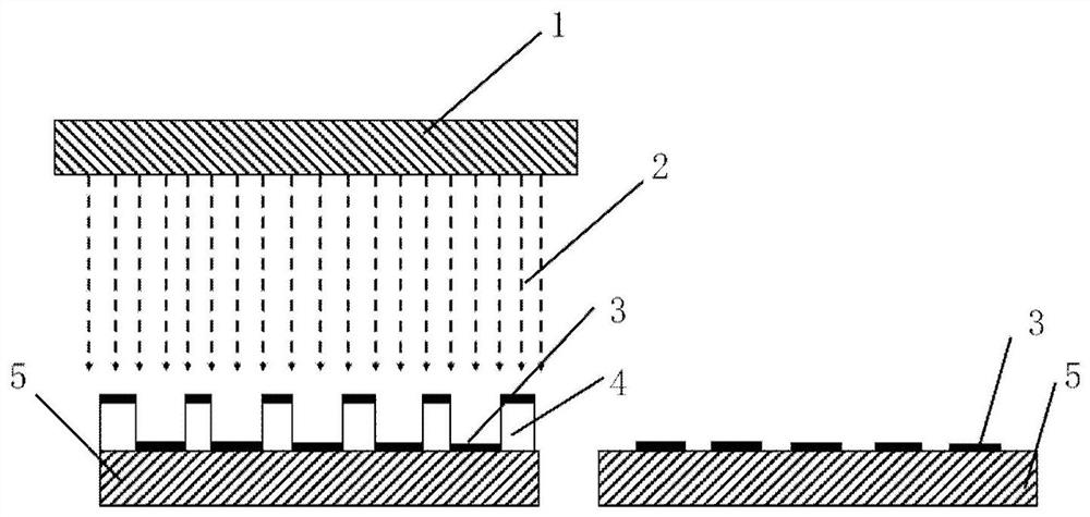
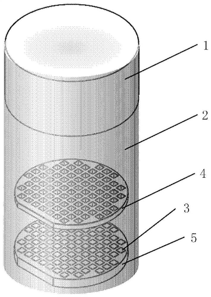
[0023] Align the openings on the prepared mask with the sensitive areas of the substrate;

[0024] Inject the precursor solution of the sensitive material to be coated onto the nozzle;

[0025] Set the nozzle operating parameters;

[0026] Aim the...


PUM


Abstract

The invention relates to a spraying method of a wafer-level sensitive material and a semiconductor sensor. The spraying method of the wafer-level sensitive material comprises the following steps thata hole in a prepared mask plate is aligned with a sensitive area of a substrate; a precursor solution of the sensitive material to be coated is injected onto a spray head; spray head operation parameters are set; the spray head is aligned with the mask plate to start spraying; and after the spraying is finished, the mask plate is separated from the substrate to obtain the wafer-level sensitive material. According to the spraying method of the wafer-level sensitive material and the semiconductor sensor, by adopting a high-precision mask and combining a large-area spraying method, wafer level one-time uniform modification and fixation of a nanometer gas sensitive material can be realized; the spraying method is adopted, and the film forming thickness of the sensitive material can be accurately controlled by calculating the spraying time; by adopting a high-precision mask technology, a non-sensitive area can be perfectly protected from being polluted by the sensitive material so that a subsequent packaging process cannot be affected; and therefore by adopting the method, perfect compatibility with the subsequent process is achieved.

Description

technical field [0001] The invention belongs to the field of sensors, and in particular relates to a wafer-level sensitive material and a spraying method for semiconductor sensors. Background technique [0002] The micro metal oxide semiconductor sensor (MOS) based on nano-sensitive materials is a sensor with small size, low power consumption, high sensitivity, low price and good selectivity. This sensor, because of its low price and wide range of gas detection (the corresponding sensitive film can be selected according to the gas composition to realize multiple gas detection), is widely used in the monitoring of toxic gases in industrial parks, monitoring of industrial boilers and automobile exhaust emissions, furniture and It is widely used in fields such as monitoring of toxic and harmful gases released by building materials. [0003] However, the modification and fixation of the sensitive materials of the existing metal oxide detectors are not at the wafer level. The ba...

Claims


Application Information

Patent Timeline
IPC IPC(8): B05D1/02B05D1/32
CPCB05D1/02B05D1/32B05D2203/30B05D2203/35
Inventor 孙建海马天军王海容赵玉龙
Owner AEROSPACE INFORMATION RES INST CAS
Why Eureka
Try Eureka