Thin-film resistance strain pressure sensor and layout optimization method thereof

A technology of pressure sensor and thin film resistance, which is applied in the field of thin film resistance strain pressure sensing, can solve the problems of anti-static discharge and surge current difference, unreasonable resistance wire routing, poor electromagnetic compatibility of sensor chips, etc., to achieve anti-static Strong surge capability and good dynamic signal perception ability

Active Publication Date: 2021-03-12
HUNAN QITAI INFORMATION TECH
View PDF16 Cites 0 Cited by
  • Summary
  • Abstract
  • Description
  • Claims
  • Application Information

AI Technical Summary

Problems solved by technology

However, in many existing layout schemes, the strain of the flat diaphragm is not reasonably analyzed and utilized, and the wiring of the resistance wire is unreasonable, resulting in low sensitivity of the sensor
At the same time, most of the transition connections between the resistance wires in the existing schemes use simple corners, but there are impedance mutations and parasitic capacitance and inductance at the corners, which will cause signal reflections when detecting dynamic signals, and lead to poor electromagnetic compatibility of the sensor chip. Good, poor resistance to ESD and surge current

Method used


Image

  • Thin-film resistance strain pressure sensor and layout optimization method thereof
  • Thin-film resistance strain pressure sensor and layout optimization method thereof
  • Thin-film resistance strain pressure sensor and layout optimization method thereof

Examples


Embodiment Construction

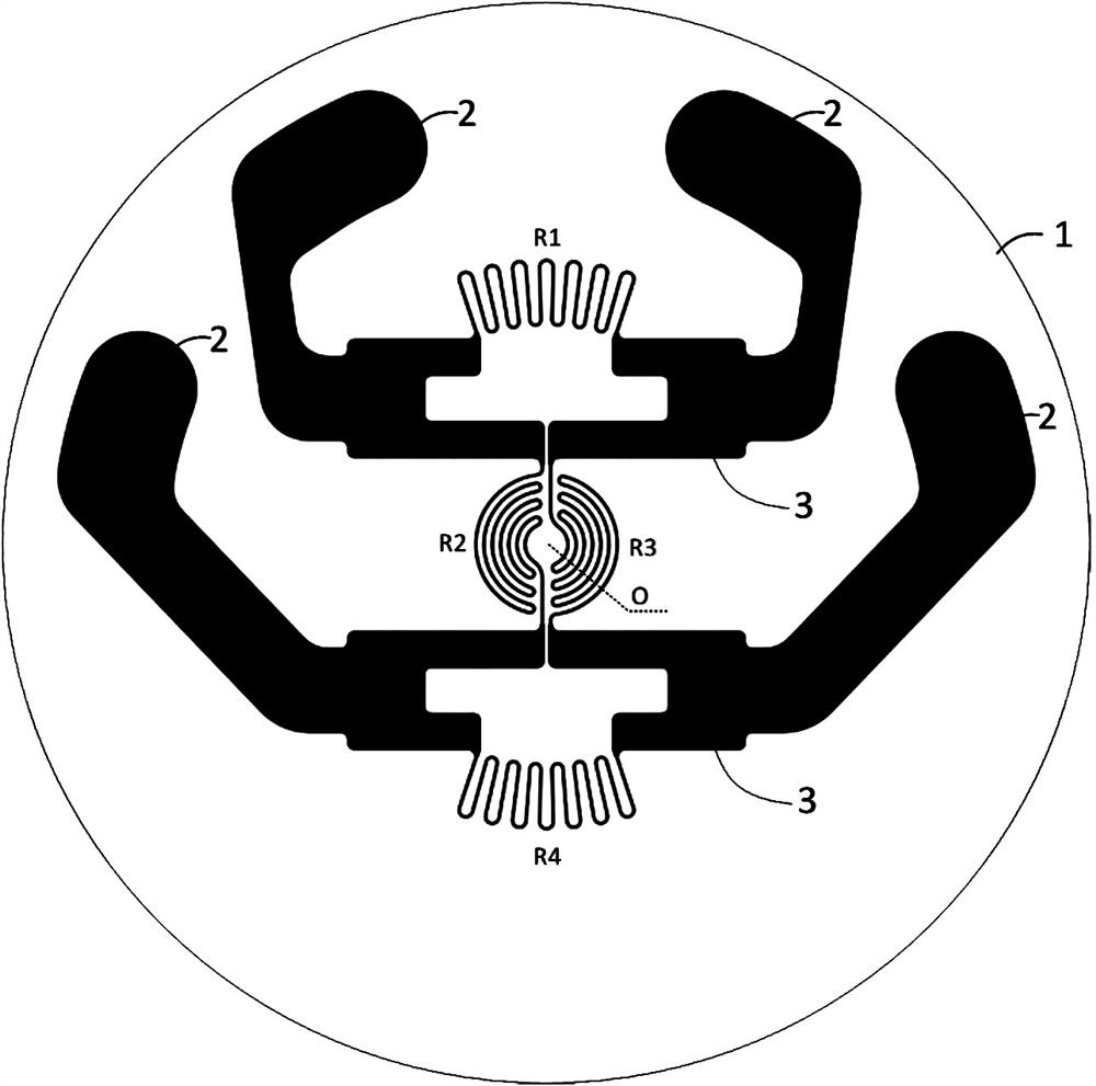
[0037] The technical problems to be solved by the present invention are: firstly, the strain magnitude and direction of each position in the sensitive deformation area on the pressure sensor chip will change, and the simple straight line and corner connection will cause the sensitivity of the sensor to fail to meet the design requirements. Problems such as poor surge capability and poor dynamic signal perception capability are solved by the present invention through reasonable layout design; the second is that the sensor chip layout is different from ordinary digital chip or digital circuit layout, and there are some irregular areas and transition connections How to accurately calculate the equivalent resistance of these components is also a technical problem to be solved by the present invention.

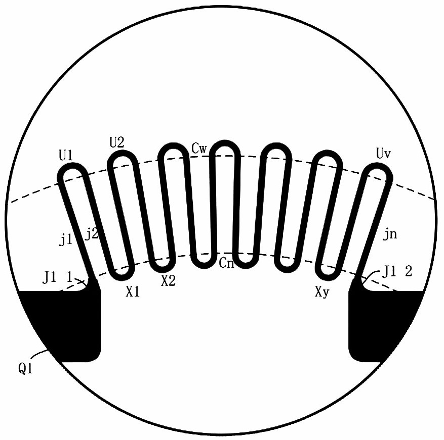
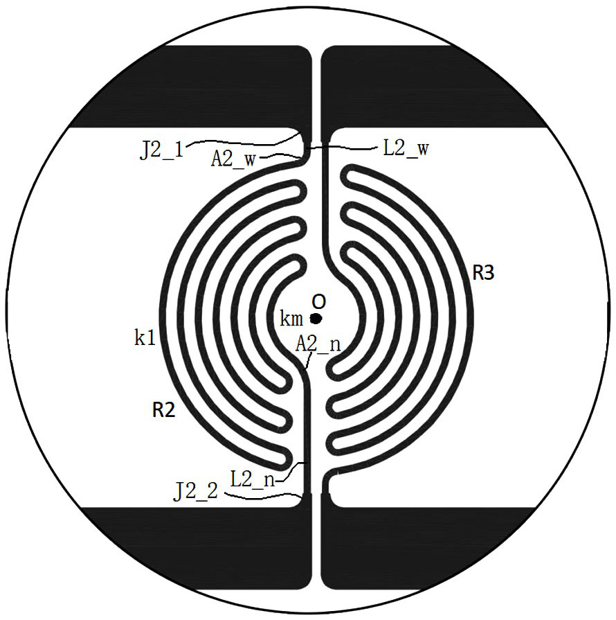
[0038] Such as figure 1 As shown, the thin-film resistive strain pressure sensor of this embodiment includes a flat diaphragm 1 and a film-shaped sensitive circuit arranged on the ...


PUM


Abstract

The invention discloses a thin-film resistance strain pressure sensor and a layout optimization method thereof. The thin-film resistance strain pressure sensor comprises a thin-film sensitive circuitdisposed on a flat diaphragm, and comprises four resistors R1 to R4 which are connected end to end to form a Wheatstone bridge. The resistor R1 and the resistor R4 are both formed by connecting n radial lines in series end to end, the extending lines of the n radial lines penetrate through the circle center O of the circular deformation area of the flat diaphragm in a radial mode, the resistor R2and the resistor R3 are both formed by connecting m tangential lines arranged around the circle center O in series end to end, and the resistor R1 and the resistor R4, and the resistor R2 and the resistor R3 are symmetrically arranged relative to the circle center O. According to the pressure sensor, the sensitivity of the sensor can meet the design requirement, the surge resistance is high, the dynamic signal sensing capability is good, and accurate bridge balance is realized; and according to the layout optimization method, the layout can be finely adjusted, and it is ensured that the layoutmeets the requirement for bridge balance.

Description

technical field [0001] The invention relates to thin film resistance strain pressure sensing technology, in particular to a thin film resistance strain pressure sensor and a layout optimization method thereof. Background technique [0002] Sensor technology, communication technology and computer technology constitute the three pillars of modern information. They respectively complete the information extraction, information transmission and information processing of the measured, which is an important part of the development of contemporary science and technology. The sensor converts environmental signals such as force, heat, light, magnetism, sound, and humidity into electrical signals for further analysis and processing. It is the main way and means to obtain information in the natural field and is the information source of the Internet of Things technology. . [0003] While sensor technology is widely used in important fields such as industrial automation, military defen...

Claims


Application Information

Patent Timeline
Patent Type & Authority Applications(China)
IPC IPC(8): G01B7/16G01L1/22
CPCG01B7/18G01L1/2262
Inventor 王国秋黄坚陈璀
Owner HUNAN QITAI INFORMATION TECH
Why Eureka
Try Eureka