Semiconductor storage device
A storage device and semiconductor technology, applied in semiconductor devices, information storage, static memory, etc., can solve the problems of voltage affecting non-selected bit lines or non-selected word lines, misapplication, etc.
- Summary
- Abstract
- Description
- Claims
- Application Information
AI Technical Summary
Problems solved by technology
Method used
Image
Examples
no. 1 Embodiment approach
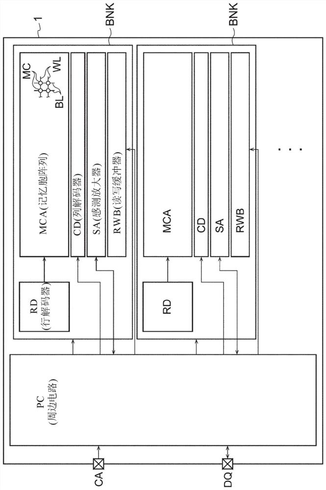
[0024] figure 1 It is a block diagram showing a configuration example of the semiconductor memory device according to the first embodiment. The semiconductor storage device 1 can be, for example, a volatile memory such as DRAM (Dynamic Random Access Memory, dynamic random access memory), a NAND (Not And, and non) type EEPROM (Electrically Erasable and Programmable Read-Only-Memory, electrically erasable Programmable read-only memory), ReRAM (Resistive Random Access Memory, resistive random access memory), MRAM (Magnetic Random Access Memory, magnetoresistive random access memory), PCM (Phase Change Memory, phase change memory), etc. volatile memory. In addition, the semiconductor memory device 1 may be, for example, one memory chip, or may be a module such as a DIMM (Dual Inline Memory Module) including a plurality of memory chips.
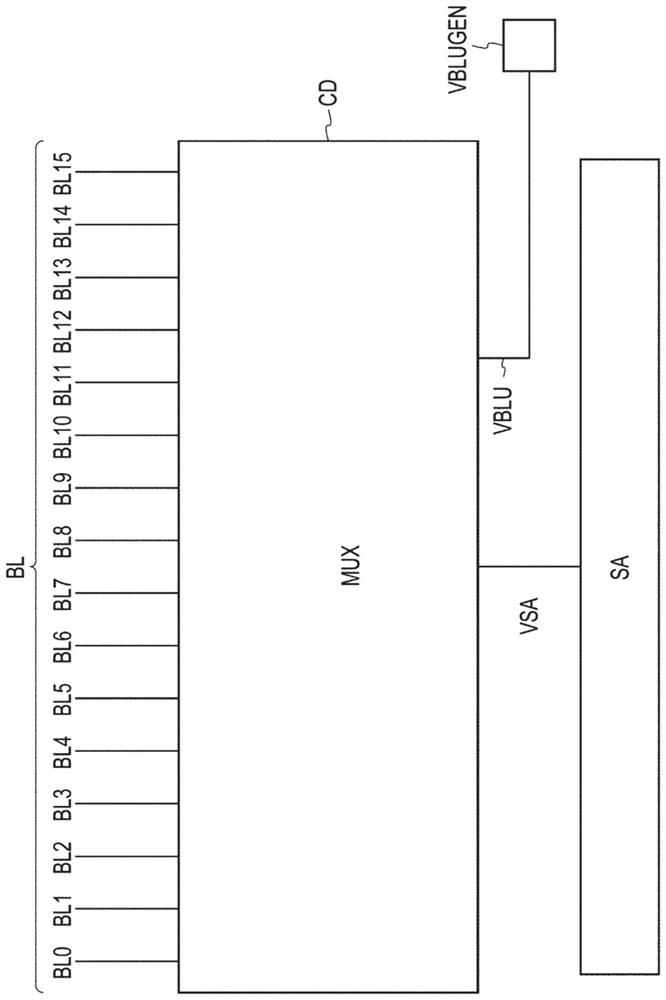
[0025] figure 1 The illustrated semiconductor memory device 1 is configured as, for example, one memory chip. Hereinafter, the semiconductor ...
no. 2 Embodiment approach
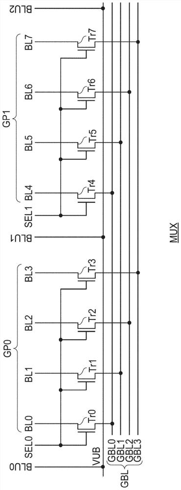
[0060] Figure 5 It is a circuit diagram showing a configuration example of the multiplexer MUX in the column decoder CD of the second embodiment. In the second embodiment, dummy bit lines are provided on both sides of each group GP0, GP1, and each group GP0, GP1 is sandwiched by two dummy bit lines. For example, dummy bit lines BLU10 and BLU11 are provided on both sides of the group GP0, and the group GP0 is sandwiched between the dummy bit lines BLU10 and BLU11. On both sides of the group GP1, there are dummy bit lines BLU12 and BLU13, and the group GP1 is sandwiched between the dummy bit lines BLU12 and BLU13.
[0061] Like the dummy bit lines BLU0 to BLU2 of the first embodiment, the dummy bit lines BLU10 to BLU13 extend along the bit lines BL0 to BL7 to a length equal to or longer than that of the bit lines BL0 to BL7 .
[0062] Transistors Tr10 to Tr13 as second transistors are connected between the dummy bit lines BLU10 to BLU13 and the non-selection signal line VUB. ...
no. 3 Embodiment approach
[0081] Figure 7It is a circuit diagram showing a configuration example of the multiplexer MUX in the column decoder CD of the third embodiment. In the third embodiment, transistors Tr10 to Tr13 as second transistors are respectively connected between the bit lines BL0 , BL3 , BL4 , and BL7 located at both ends of each of the groups GP0 and GP1 and the non-selection signal line VUB. . That is, two transistors are connected to each of the bit lines BL0, BL3, BL4, and BL7 located at both ends of each group GP0, GP1, and one transistor is connected to each of the other middle bit lines BL1, BL2, BL5, and BL6. transistor. Dummy selection signal lines SELU0 , SELU1 as second selection signal lines are provided corresponding to each of the groups GP0 , GP1 . The dummy selection signal line SELU0 is commonly connected to the gate electrodes of the transistors Tr10 and Tr11 , and the dummy selection signal line SELU1 is commonly connected to the gate electrodes of the transistors T...
PUM
 Abstract
Description
Claims
Application Information
 - R&D Engineer
- R&D Manager
- IP Professional
- Industry Leading Data Capabilities
- Powerful AI technology
- Patent DNA Extraction
Browse by: Latest US Patents, China's latest patents, Technical Efficacy Thesaurus, Application Domain, Technology Topic, Popular Technical Reports.
© 2024 PatSnap. All rights reserved.Legal|Privacy policy|Modern Slavery Act Transparency Statement|Sitemap|About US| Contact US: help@patsnap.com


