

Batch leveling and slicing device for lead frame copper strips
A lead frame and slicing device technology, which is applied in the field of lead frame copper strip batch leveling and slicing devices, can solve the problems of large limitations, uneven cutting surface, slow speed, etc., to improve the leveling quality, prevent left and right shaking, and prevent stacking Effect
- Summary
- Abstract
- Description
- Claims
- Application Information
AI Technical Summary
Problems solved by technology
Method used
Image

Examples
Embodiment 1
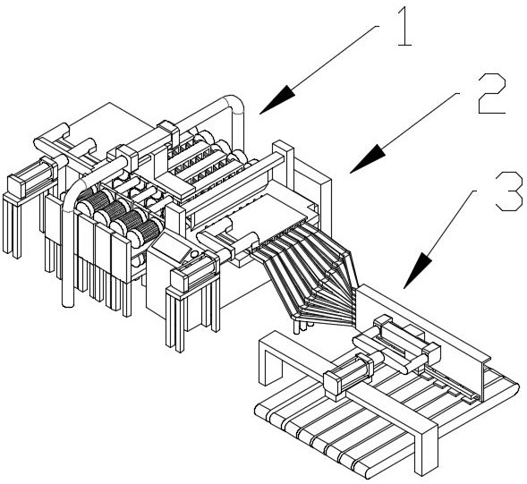
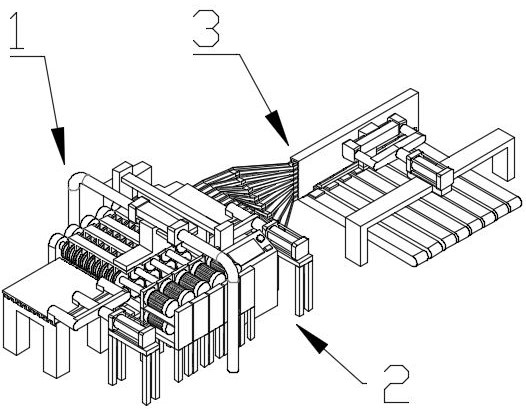
[0057] like Figure 1-Figure 17 The shown device for batch leveling and slicing of lead frame copper strips includes a leveling unit 1 and a slicing unit 2 .
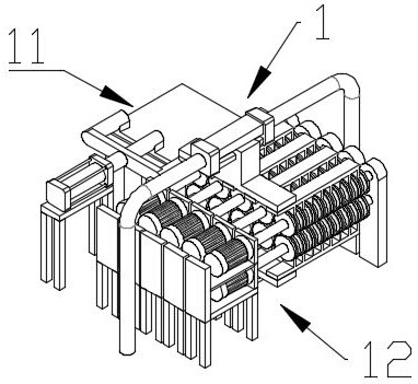
[0058] The leveling unit 1 is used for leveling the lead frame copper tape. The leveling unit 1 includes a first guide mechanism 11 and a flattening mechanism 12. The first guide mechanism 11 includes a guide table 111. The upper end surface of the guide table 111 is provided with a plurality of first guide mechanisms. A guide groove 1111, one end of the guide table 111 is provided with a first bracket 1121 at a predetermined distance. A lateral plate 1122 is provided with a plurality of first branch rods 1123 on one side, one end of the first branch rod 1123 is provided with a first guide plate 113 at the lower end of the outer circumference side, and a plurality of first guide grooves 1111 are arranged on the bottom end of the first guide plate 113 in an array. The first guide strip 1131 is used to limit the copper s...
Embodiment 2
[0064] like Figure 1-Figure 27 The shown device for batch leveling and slicing of lead frame copper strips includes the batch leveling and slicing device for lead frame copper strips of the first embodiment, and a steering collection unit 3 .
[0065] The turning and collecting unit 3 is set at one end of the slicing unit 2. The turning and collecting unit 3 includes a transfer mechanism 31, an arrangement mechanism 32, a translation mechanism 33, and a transfer mechanism 34. The transfer mechanism 31 includes a plurality of fifth brackets 3111 arranged in an array, and the fifth brackets 3111 The upper end is provided with a slideway 311 for sliding the copper sheet. The slideway 311 is a ramp whose height decreases from the feed end to the feed end. The feed end of the slideway 311 is set at the feed end of the second guide groove 2151, and the feed end of the slideway 311 is vertical. The arrangement is arranged in a straight array. The arrangement mechanism 32 is arranged...
PUM
 Abstract
Description
Claims
Application Information