ZnSe substrate 7.7-9.5micrometer waveband high-durability antireflection film and preparation method

A durable and anti-reflection film technology, which is applied in ion implantation plating, coating, instruments, etc., can solve the problem of weak anti-salt solution immersion and anti-friction ability, and cannot well meet the requirements of new optical instruments, optical Poor performance and other problems, to improve the ability of anti-salt solution corrosion and anti-friction, improve transmittance, enhance compactness and mechanical strength

Inactive Publication Date: 2021-03-16
YUNNAN KIRO CH PHOTONICS
View PDF5 Cites 9 Cited by
  • Summary
  • Abstract
  • Description
  • Claims
  • Application Information

AI Technical Summary

Problems solved by technology

[0003] The invention provides a ZnSe base 7.7-9.5 μm band anti-reflection film with high durability and a preparation method, which is used to solve the poor optical performance of the ZnSe material base 7.7-9.5 μm band anti-reflection film in the prior art and resistance to salt solution Soaking and anti-friction ability is not strong, so it can't meet the technical problems of the use requirements of new optical instruments

Method used


Image

  • ZnSe substrate 7.7-9.5micrometer waveband high-durability antireflection film and preparation method
  • ZnSe substrate 7.7-9.5micrometer waveband high-durability antireflection film and preparation method
  • ZnSe substrate 7.7-9.5micrometer waveband high-durability antireflection film and preparation method

Examples


Embodiment 1

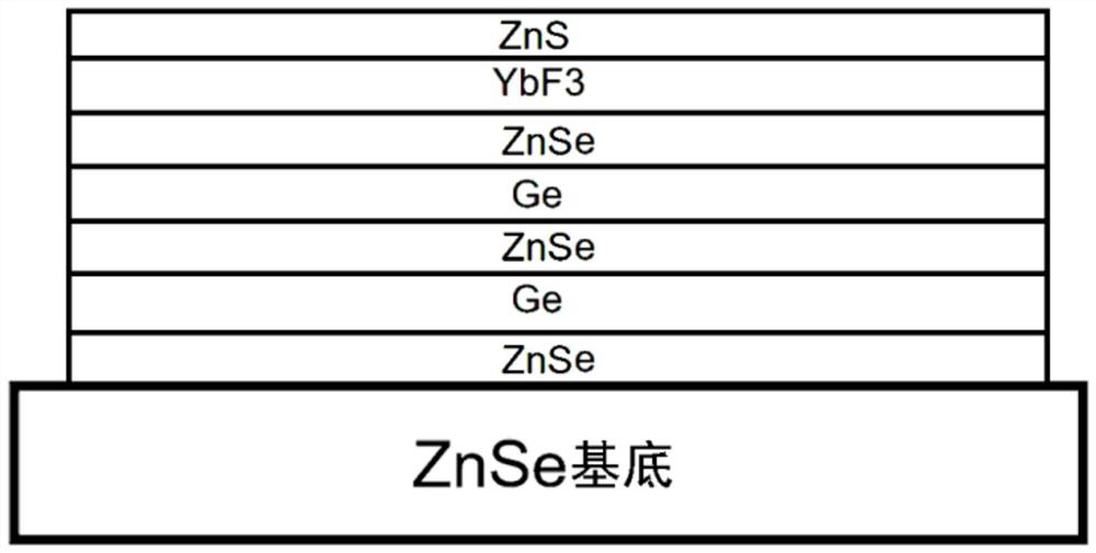
[0024] Choose Φ37.5mm ZnSe material lens, in the range of 7.7-9.5μm for the surface layer of the substrate, use APS ion source, fill with argon gas, gas flow rate 10sccm, bias voltage 120V, discharge voltage 80V, discharge Current 30A, coil current 2A, bombardment 6min; at 140°C, use APS ion source assisted deposition method, fill in argon gas, fill in argon gas, gas flow rate 10sccm, bias voltage 120V, discharge voltage 80V, discharge current 35A, Coil current 2A, sequentially plating a ZnSe layer with a thickness of 50nm, a Ge layer with a thickness of 122.05nm, a ZnSe layer with a thickness of 679.67nm, a Ge layer with a thickness of 154.76nm, a ZnSe layer with a thickness of 230.54nm, a YbF3 layer with a thickness of 840.00nm, and a thickness of 255nm ZnS layer; use the RF radio frequency source of the plasma chemical vapor deposition coating equipment, fill it with argon gas, the gas flow rate is 150sccm, and the power is 400W, and plasma bombards the film layer for 20 min...

Embodiment 2

[0029] Choose Φ26mm×2mm planar ZnSe material parts, use APS ion source for the surface layer of one surface of the substrate in the range of 7.7-9.5μm, fill with argon gas, gas flow rate 9sccm, bias voltage 125V, discharge voltage 90V, Discharge current 40A, coil current 4A, bombardment 6min; at 130°C, use APS ion source assisted deposition method, fill with argon gas, fill with argon gas, gas flow rate 9sccm, bias voltage 125V, discharge voltage 90V, discharge current 40A , coil current 4A, sequentially plating a ZnSe layer with a thickness of 50nm, a Ge layer with a thickness of 122.05nm, a ZnSe layer with a thickness of 679.67nm, a Ge layer with a thickness of 154.76nm, a ZnSe layer with a thickness of 230.54nm, a YbF3 layer with a thickness of 840.00nm, a thickness of 255nm ZnS layer; use the RF radio frequency source of the plasma chemical vapor deposition coating equipment, fill it with argon gas, the gas flow rate is 200sccm, the power is 500W, and plasma bombards the fi...

Embodiment 3

[0034] Select Φ40mm×3mm planar ZnSe material parts, use APS ion source for the surface layer of one surface of the substrate in the range of 7.7-9.5μm, fill with argon gas, gas flow rate 8sccm, bias voltage 120V, discharge voltage 70V, Discharge current 25A, coil current 2A, bombardment 6min; at 150°C, use APS ion source assisted deposition method, fill with argon gas, fill with argon gas, gas flow rate 10sccm, bias voltage 120V, discharge voltage 70V, discharge current 30A , coil current 2A, sequentially plating a ZnSe layer with a thickness of 50nm, a Ge layer with a thickness of 122.05nm, a ZnSe layer with a thickness of 679.67nm, a Ge layer with a thickness of 154.76nm, a ZnSe layer with a thickness of 230.54nm, a YbF3 layer with a thickness of 840.00nm, a thickness of 255nm ZnS layer; use the RF radio frequency source of plasma chemical vapor deposition coating equipment, fill with argon gas, gas flow rate 100sccm, power 400W, plasma bombardment on the film layer, bombardm...


PUM

PropertyMeasurementUnit
thicknessaaaaaaaaaa
thicknessaaaaaaaaaa
thicknessaaaaaaaaaa

Abstract

The invention relates to the technical field of infrared coating, in particular to a ZnSe substrate 7.7-9.5micrometer waveband high-durability antireflection film and a preparation method. The ZnSe substrate 7.7-9.5micrometer waveband high-durability antireflection film is a film layer structure arranged on the surface of a base layer and contacted with air, and is composed of a ZnSe layer, a Ge layer, a ZnSe layer, a Ge layer, a ZnSe layer, a YbF3 layer and a ZnS layer that are stacked and connected sequentially. The ZnSe substrate 7.7-9.5micrometer waveband high-durability antireflection film disclosed by the invention is used for solving the technical problems that in the prior art, a ZnSe material substrate 7.7-9.5micrometer waveband antireflection film is poor in optical performance,poor in salt solution soaking resistance and friction resistance and incapable of well meeting the use requirements of a novel optical instrument.

Description

technical field [0001] The invention relates to the technical field of infrared coating, in particular to a ZnSe substrate 7.7-9.5 μm band high-durability anti-reflection film and a preparation method. Background technique [0002] As a material with good optical transparency in the infrared band, ZnSe is widely used in infrared optical systems. With the continuous development of infrared optical instruments, the requirements for the imaging quality of optical systems are also getting higher and higher. The ZnSe material used in the past is based on the 7.7-9.5μm band anti-reflection film, and the average transmittance in the band is about 98%. Requirements for the use of the latest infrared optical systems. Contents of the invention [0003] The invention provides a ZnSe base 7.7-9.5 μm band anti-reflection film with high durability and a preparation method, which is used to solve the poor optical performance of the ZnSe material base 7.7-9.5 μm band anti-reflection fil...

Claims


Application Information

Patent Timeline
Patent Type & Authority Applications(China)
IPC IPC(8): G02B1/115C23C14/58C23C14/28C23C14/18C23C14/06
CPCG02B1/115C23C14/0623C23C14/18C23C14/0694C23C14/28C23C14/5833
Inventor 李刚董力张友良杨伟声张红梅吴栋才耿曙王宇彤
Owner YUNNAN KIRO CH PHOTONICS
Why Eureka
Try Eureka