System-on-chip development environment building method and system

A development environment and component technology, applied in the direction of creating/generating source code, program control design, program loading/starting, etc., to achieve the effect of good application prospects, convenient construction process, and ensure system stability

Active Publication Date: 2021-03-16
CHINA NAT DIGITAL SWITCHING SYST ENG & TECHCAL R&D CENT +1
View PDF8 Cites 0 Cited by
  • Summary
  • Abstract
  • Description
  • Claims
  • Application Information

AI Technical Summary

Problems solved by technology

[0003] Data processing based on chip design has a good development prospect, but its huge computing resources and complex interconnection bring great challenges to the compil

Method used


Image

  • System-on-chip development environment building method and system
  • System-on-chip development environment building method and system
  • System-on-chip development environment building method and system

Examples


Embodiment Construction

[0028] In order to make the purpose, technical solution and advantages of the present invention more clear and understandable, the present invention will be further described in detail below in conjunction with the accompanying drawings and technical solutions.

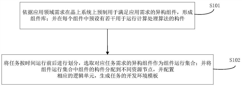
[0029] The system on chip integrates the system in a single chip, and its core function lies in the integration of multi-functional modules. The technical advantage is mainly compared with SoC chips and PCB-based integration technologies. Come change. The on-chip system has a good development prospect, but its huge computing resources and complex interconnection have brought great challenges to the compilation system. How to make full use of system resources and provide users with a convenient and easy-to-use development environment. Embodiment of the present invention, see figure 1 As shown, a method for building an on-chip system development environment is provided, see figure 1 As shown, it contains the following...


PUM


Abstract

The invention belongs to the technical field of computer processing, and particularly relates to a system-on-chip development environment building method and system, and the method comprises the steps: prefabricating a heterogeneous assembly for meeting an application demand on a system-on-chip according to the demands of an application field, and forming an assembly library; wherein a plurality of components used for operating a calculation processing algorithm are preset in each assembly; dividing tasks according to time before and after running, and selecting heterogeneous components corresponding to task requirements as a component running set; and allocating components of the components in the assembly running set to different resource nodes, and configuring corresponding logic unitsto generate a development environment template of the task. Core particles with the processing function serve as components in the development assembly, each PE unit can be achieved corresponding to one component, different assemblies are preset according to field requirements, the whole building process is convenient and fast, reuse of various assemblies is facilitated, the assemblies can be usedfor more flexibly meeting new application requirements, and the development efficiency is improved. Good application prospects are realized.

Description

technical field [0001] The invention belongs to the technical field of computer processing, and in particular relates to a method and system for building an on-chip system development environment. Background technique [0002] In 2017, DARPA (Defense Advanced Research Projects Agency) of the United States planned a chiplet project named "Common Heterogeneous Integration and IP Reuse Strategies (CHIPS)" in the "Electronic Renaissance Program", and the participants included Intel. , Micron, Cadence, Synopsys, etc. It is a type of die that satisfies specific functions and can be called a module chip. Chiplet mode is a mode in which multiple module chips and underlying basic chips are packaged together through die-to-die interconnection technology to form a multi-functional heterogeneous System in Packages (SiPs) chip. In recent years, chiplet (Chiplet) has become a hot word in the semiconductor industry. When Moore's Law is running towards the physical limit of 7nm, 3nm, and...

Claims


Application Information

Patent Timeline
IPC IPC(8): G06F8/34G06F8/35G06F9/445
CPCG06F8/34G06F8/35G06F9/44526
Inventor 邬江兴刘勤让魏帅沈剑良汤先拓吕平李沛杰陈艇刘冬培董春雷
Owner CHINA NAT DIGITAL SWITCHING SYST ENG & TECHCAL R&D CENT
Why Eureka
Try Eureka