
Interlayer connection of stacked microelectronic components

A technology of interlayer connection and microelectronics, applied in the direction of electrical components, electrical solid devices, semiconductor/solid device parts, etc., can solve impractical problems

Pending Publication Date: 2021-03-16
隔热半导体粘合技术公司
View PDF3 Cites 0 Cited by
  • Summary
  • Abstract
  • Description
  • Claims
  • Application Information

AI Technical Summary

Problems solved by technology

However, this solution may become impractical if stacking more than 2 or 3 dies due to the additional TSVs used for the connections

Method used


Image

  • Interlayer connection of stacked microelectronic components
  • Interlayer connection of stacked microelectronic components
  • Interlayer connection of stacked microelectronic components

Examples


Embodiment Construction

[0030] overview

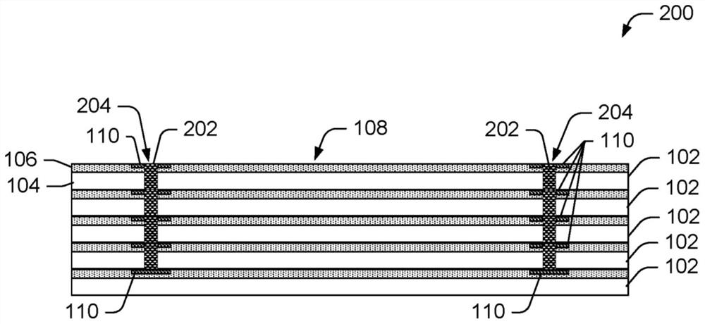
[0031] In various embodiments, techniques and devices may be employed to simplify the common electrical connection of all desired dies and / or wafers in a die-to-die stack, a die-to-wafer stack, or a wafer-to-wafer stack, particularly when the stack 2 1 or more dies and / or wafers. Discussions herein in relation to dies also refer to wafers or other substrates in such stacks.

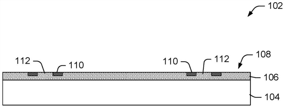
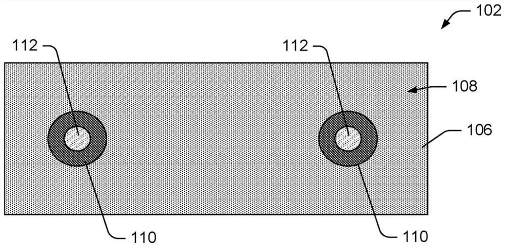
[0032] see Figure 1A (which shows a cross-sectional profile view) and Figure 1B (which shows a top view), the patterned metal and oxide layers are often used as hybrid bonds, or The surface layer is disposed on a die, wafer, or other microelectronic substrate (hereinafter referred to as "die 102"). A representative device die 102 may be formed using various techniques to include a base substrate 104 and one or more insulating or dielectric layers 106 . The base substrate 104 may be composed of silicon, germanium, glass, quartz, a dielectric surface, a direct gap semiconductor mater...


PUM


Abstract

Representative techniques and devices including process steps may be employed to form a common interconnection of a multi-die or multi-wafer stack. Each device of the stack includes a conductive pad disposed at a predetermined relative position on a surface of the device. The devices are stacked to vertically align the conductive pads. A through-silicon via is formed that electrically couples theconductive pads of each device of the stack.

Description

[0001] Priority claims and cross-references to related applications [0002] This application claims U.S. Nonprovisional Application No. 16 / 438,714, filed June 12, 2019, and U.S. Provisional Application No. 62 / 683,857, filed June 12, 2018, pursuant to 35 U.S.C. § 119(e)(1) interests, the entire contents of which are incorporated herein by reference. technical field [0003] The following description refers to an integrated circuit ("IC"). More specifically, the following description relates to the fabrication of IC dies and wafers. Background technique [0004] Microelectronic components typically include thin plates (commonly referred to as semiconductor wafers) formed of semiconductor material such as silicon or gallium arsenide. A wafer may be formed to include a plurality of integrated chips or dies located on a surface of the wafer and / or partially embedded within the wafer. Dies separated from the wafer are typically provided as individual, pre-packaged units. In ...

Claims


Application Information

Patent Timeline
IPC IPC(8): H01L23/485H01L23/48H01L23/498H01L23/00H01L25/07H01L21/768
CPCH01L23/481H01L25/0657H01L2225/06544H01L2225/06593H01L23/544H01L2223/54426H01L2223/5442H01L2224/9202H01L24/82H01L24/24H01L2224/24145H01L2224/24051H01L25/50H01L24/80H01L24/08H01L2224/08145H01L2224/73201H01L2224/73251H01L2224/9212H01L2224/9222H01L2224/821H01L24/92H01L24/73H01L2224/94H01L24/94H01L2224/92H01L2224/80121H01L2224/08H01L2224/24H01L2224/80H01L2224/82H01L2924/00012H01L21/304H01L21/76898H01L2924/00014H01L2224/08146H01L24/89H01L24/05H01L2224/05552H01L2225/06562H01L2224/80896H01L2224/0557H01L2224/80895H01L2224/05647H01L2224/03616H01L24/03
Inventor G·高B·哈巴
Owner 隔热半导体粘合技术公司
Learn More