Spacer for optical device lens and method for manufacturing same

A technology for optical instruments and manufacturing methods, applied to optical components, instruments, optics, etc., can solve problems such as glare, burrs, and large thickness deviations, and achieve scratch resistance, improved chemical resistance, and excellent processability Effect

Pending Publication Date: 2021-03-19
TAIYO INK MFG CO KOREALTD
View PDF6 Cites 0 Cited by
  • Summary
  • Abstract
  • Description
  • Claims
  • Application Information

AI Technical Summary

Problems solved by technology

[0012] However, conventional spacers have the following problems: glare, burrs, poor hygroscopicity, chemical resistance,

Method used


Image

  • Spacer for optical device lens and method for manufacturing same
  • Spacer for optical device lens and method for manufacturing same
  • Spacer for optical device lens and method for manufacturing same

Examples


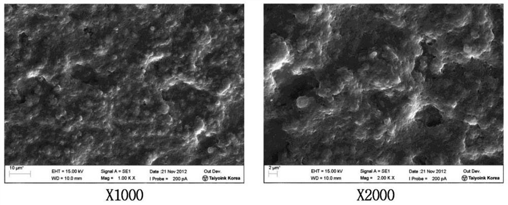
manufacture example 1

[0063] 1. The composition for the organic layer of this invention which consists of the following components was prepared.

[0064] Table 1

[0065]

[0066]

[0067] 2. The prepared above-mentioned composition was coated on a copper foil having a thickness of 18 μm by micro gravure coating (Micro Gravure Coating).

[0068] 3. In a box oven, dry with hot air at a temperature of 45° C. for 6 hours, and heat cure at a temperature of 150° C. for 30 minutes, thereby forming an organic layer with a film thickness of 4±1 μm.

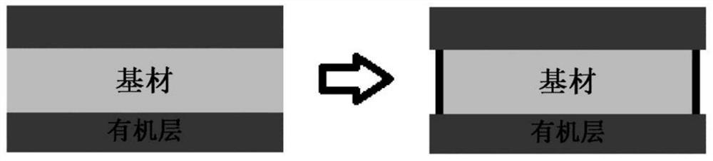
[0069] 4. After processing (punching) the base material on which the organic layer formed of the cured composition was formed through a circular through-hole, an annular spacer was manufactured.

[0070] 5. After immersing the above-mentioned spacer in the oxidation treatment chemical solution (LDB A, LDB B of YMT Company) for 10 minutes to form an oxide coating film on the exposed copper, wash with water to remove the chemical solution.

[0071] 6. Af...

manufacture example 2

[0073] A conventional film-type separator was manufactured by the following method.

[0074] 1. A conventional coating liquid for light-shielding formation of a film-type spacer containing the following components was prepared.

[0075] Table 2

[0076] Element Content (parts by weight) Hydroxy acrylic acid (50% by weight of solid content) 153.8 Isocyanate (75% by weight of solid content) 30.8 Carbon black (black chlorinated carbon, solid content weight 100%) 24 Silica (average particle size 5μm) 3.0 Methyl ethyl ketone, toluene (solvent) 611.4~1091.4

[0077] 2. The prepared coating liquid for light-shielding formation was coated on black polyethylene terephthalate having a thickness of 25 μm by microgravure coating.

[0078] 3. Drying with hot air at a temperature of 45° C. for 24 hours in a box oven, thereby forming an organic layer with a film thickness of 3±1 μm.

[0079] 4. After processing the hardened spacer light-shieldi...

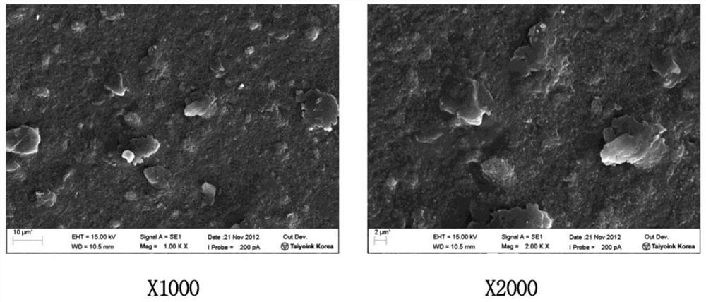
manufacture example 3

[0081] A conventional copper or copper alloy spacer was produced by the following method.

[0082] 1. Through the circular through hole, the copper plate with a thickness of 0.035mm was used to manufacture the annular spacer.

[0083] 2. Surface treatment was carried out by immersion in a sulfuric acid solution (10 wt %) for 2 minutes.

[0084] 3. The spacer was immersed for 10 minutes in a treatment solution to which an oxidation treatment solution (LDB A, LDB B from YMT Co., Ltd.) was added.

[0085] 4. The spacer was washed with water, and dried in an oven at a temperature of 90° C. to complete the manufacture.


PUM

PropertyMeasurementUnit
The average particle sizeaaaaaaaaaa
Thicknessaaaaaaaaaa
Thicknessaaaaaaaaaa

Abstract

The present invention relates to a spacer for optical device lens and a method for manufacturing same. The purpose of the present invention is to provide a spacer which is inexpensive, can prevent lens flare, has low hygroscopicity, chemical resistance, thickness uniformity, easy processability, and improved production convenience, can be implemented with various thicknesses, and has an excellentsurface strength. Further, the spacer of the present invention has advantages of inexpensiveness, lens flare prevention, low hygroscopicity, chemical resistance, thickness uniformity, easy processability, improved production convenience, implementation with various thicknesses, and an excellent surface strength.

Description

technical field [0001] The present invention relates to a spacer for an optical instrument lens and a manufacturing method thereof, and more particularly, to a spacer capable of preventing glare and having excellent chemical resistance and surface strength, and a manufacturing method thereof. Background technique [0002] Recently, not only camera modules are installed in cameras, but also camera modules are installed in optical devices such as smartphones, notebook PCs, and tablet PCs. The above-mentioned camera module includes a plurality of lenses, and a spacer is provided between the lenses. [0003] Generally, a spacer for an optical instrument lens is provided between lenses to maintain a space between lenses. Usually, the above-mentioned spacer is formed by coating with an opaque material in order to block light. [0004] For example, conventional film-type spacers are manufactured by coating black polyethylene terephthalate (PET) with an organic coating film. Speci...

Claims


Application Information

Patent Timeline
IPC IPC(8): G02B3/00G02B1/00
CPCG02B3/00G02B1/00
Inventor 林石峰权钟哲韩友泽
Owner TAIYO INK MFG CO KOREALTD
Why Eureka
Try Eureka