Eureka AIR delivers breakthrough ideas for toughest innovation challenges, trusted by R&D personnel around the world.

Circuit simulation method and device, electronic equipment and computer readable storage medium

A circuit simulation and circuit technology, applied in the direction of CAD circuit design, computer-aided design, calculation, etc., can solve the problem of slow simulation speed of the power network, and achieve the effect of reducing resource consumption, reducing parasitic parameters, and improving efficiency

Active Publication Date: 2021-03-26
HYGON INFORMATION TECH CO LTD
View PDF4 Cites 4 Cited by
  • Summary
  • Abstract
  • Description
  • Claims
  • Application Information

AI Technical Summary

Problems solved by technology

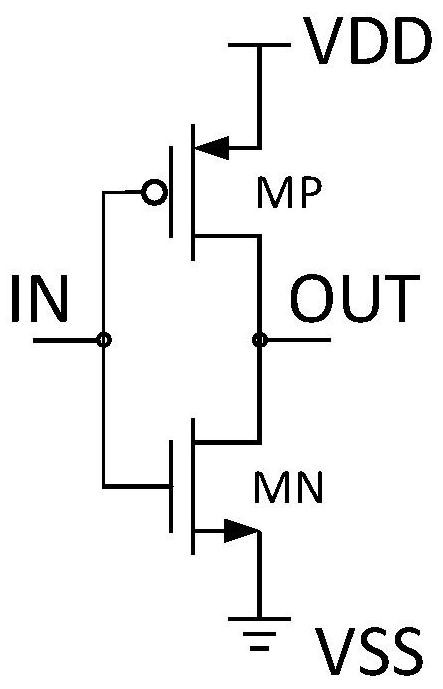
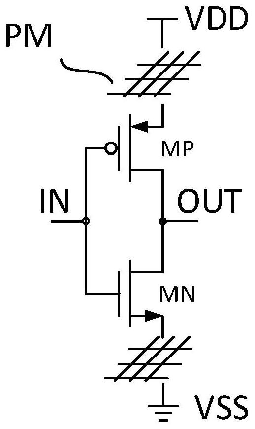
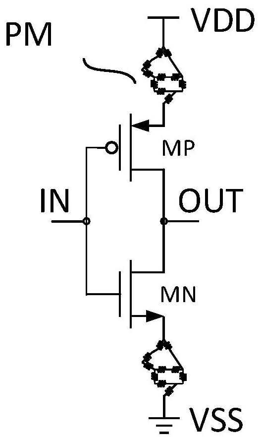
[0004] The purpose of this application is to provide a circuit simulation method, device, electronic equipment and computer-readable storage medium, which can solve the problem of slow simulation speed of the network with power supply

Method used


Image

  • Circuit simulation method and device, electronic equipment and computer readable storage medium
  • Circuit simulation method and device, electronic equipment and computer readable storage medium
  • Circuit simulation method and device, electronic equipment and computer readable storage medium

Examples


Embodiment 1

[0058] Such as figure 2 Shown is a block diagram of the electronic device. The electronic device 100 may include a memory 111 and a processor 113 . Those of ordinary skill in the art can understand that, figure 2 The shown structure is only for illustration, and does not limit the structure of the electronic device 100 . For example, the electronic device 100 may also include a ratio figure 2 more or fewer components than shown in, or with figure 2 Different configurations are shown.

[0059] The aforementioned components of the memory 111 and the processor 113 are electrically connected to each other directly or indirectly to realize data transmission or interaction. For example, these components can be electrically connected to each other through one or more communication buses or signal lines. The aforementioned processor 113 is used to execute the executable modules stored in the memory.

[0060] Wherein, the memory 111 can be, but not limited to, random access ...

Embodiment 2

[0064] see image 3 , is a flow chart of the circuit simulation method provided by the embodiment of the present application. The following will be image 3 The specific process shown will be described in detail.

[0065] In step 201, the estimated power supply voltage data determined according to the target simulation circuit is acquired.

[0066] In this embodiment, the target simulation circuit includes a power supply simulation circuit and a function simulation circuit.

[0067] In this embodiment, multiple transmission gates may be included in the functional simulation circuit. The supply voltage of the MOS connections in each transmission gate may be the same. The supply voltages of the MOS connections in the individual transmission gates can also be different.

[0068] Optionally, before the functional simulation circuit of the target simulation circuit is simulated for the first time, the estimated power supply voltage data may be determined by performing simulati...

Embodiment 3

[0109] Based on the same application concept, the embodiment of the present application also provides a circuit simulation device corresponding to the circuit simulation method. Since the problem-solving principle of the device in the embodiment of the present application is similar to the foregoing circuit simulation method embodiment, so in this embodiment For the implementation of the device, reference may be made to the description in the embodiments of the above method, and repeated descriptions will not be repeated.

[0110] see Figure 5 , is a schematic diagram of the functional modules of the circuit simulation device provided in the embodiment of the present application. Each module in the circuit simulation device in this embodiment is used to execute each step in the above method embodiment. The circuit simulation device includes: a data acquisition module 301 and a circuit simulation module 302; wherein,

[0111] A data acquisition module 301, configured to acqu...


PUM


Abstract

The invention provides a circuit simulation method and device, electronic equipment and a computer readable storage medium, and the method comprises the steps: obtaining estimated power supply voltagedata determined according to a target simulation circuit comprising a power supply simulation circuit and a function simulation circuit; and performing simulation according to the estimated power supply voltage data and the function simulation circuit to obtain a parasitic parameter netlist of the target simulation circuit. Through the method in the embodiment of the invention, the circuit simulation efficiency can be improved.

Description

technical field [0001] The present application relates to the technical field of circuit design, in particular, to a circuit simulation method, device, electronic equipment and computer-readable storage medium. Background technique [0002] Random chip technology is getting higher and higher, and chip design is becoming more and more complex. The power supply connected to the source of the MOS tube needs to be connected through multiple layers of metal or semiconductor levels, resulting in the resistance formed by the power supply network being too large to be ignored. [0003] Therefore, for the accuracy of circuit simulation, the existing circuit simulation needs to include the parasitic parameters of the power network for simulation. However, due to the relatively complex parasitic parameters of the power network, the time of circuit simulation and the consumption of machine resources have greatly increased. Contents of the invention [0004] The purpose of the present...

Claims


Application Information

Patent Timeline
Patent Type & Authority Applications(China)
IPC IPC(8): G06F30/32G06F30/337G06F115/10
CPCG06F30/32G06F30/337G06F2115/10Y02E60/00
Inventor 黄瑞锋
Owner HYGON INFORMATION TECH CO LTD
Why Eureka
Eureka Blog
Learn More