Low-dark-current image sensor pixel structure

An image sensor, pixel structure technology, applied in the direction of electric solid devices, circuits, electrical components, etc., can solve problems such as bound electrons, and achieve the effect of reducing dark current

Pending Publication Date: 2021-03-26
WILL SEMICON (SHANGHAI) CO LTD
View PDF0 Cites 3 Cited by
  • Summary
  • Abstract
  • Description
  • Claims
  • Application Information

AI Technical Summary

Problems solved by technology

[0005] The gate oxide layer (oxide) is difficult to effectively bind the electrons generated by the unsaturated dangling bonds and defects on the surface of the photodiode and its transmission channel, resulting in the generation of dark current

Method used


Image

  • Low-dark-current image sensor pixel structure
  • Low-dark-current image sensor pixel structure

Examples


Embodiment Construction

[0014] The embodiments of the present invention will be further described in detail below. The content not described in detail in the embodiments of the present invention belongs to the prior art known to those skilled in the art.

[0015] The image sensor pixel structure of low dark current of the present invention, its preferred embodiment is:

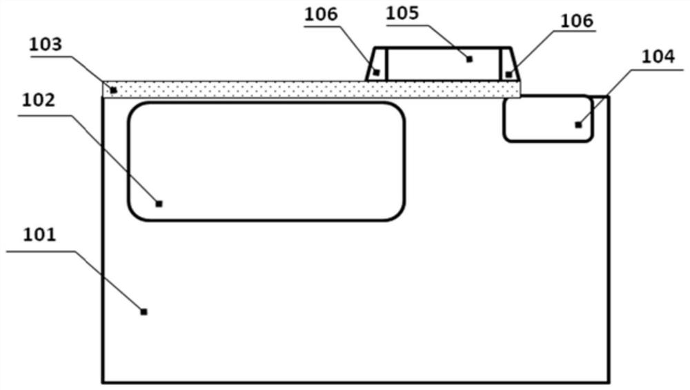
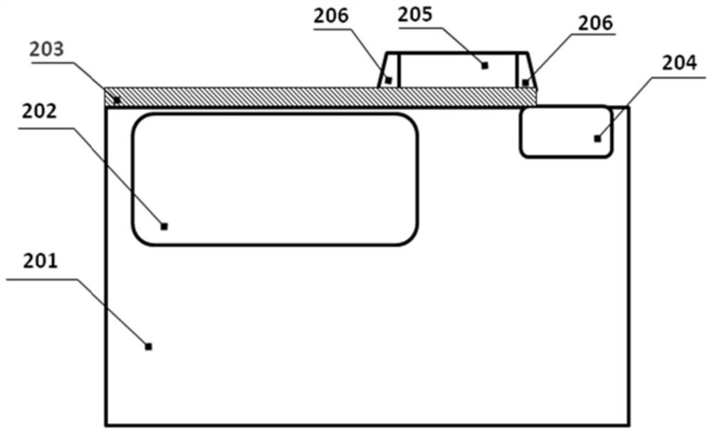
[0016] It includes a photosensitive diode and a suspended drain area placed in a semiconductor base body. A negative charge fixing medium layer is provided on the surface of the semiconductor base body. A transfer tube gate and sidewalls are arranged on the negative charge fixing medium layer.

[0017] The negative charge fixing layer is composed of an oxide layer with a high k value, and the oxide layer with a high k value is made of Al 2 o 3 , HfO 2 and / or Ta0 2 Material.

[0018] The semiconductor substrate adopts a silicon substrate, and the high-k oxide layer is deposited on the surface of the silicon substrate, and directl...


PUM


Abstract

The invention discloses a low-dark-current image sensor pixel structure. The low-dark-current image sensor pixel structure comprises a photosensitive diode, a negative charge fixing dielectric layer,a suspension drain region, a transmission tube grid and a side wall of the transmission tube grid which are arranged in a semiconductor substrate. The negative charge fixing layer is composed of an oxide layer with a high dielectric constant (k), the oxide layer with a high k value can be made of Al2O3, HfO2, Ta02 and other materials, and the oxide layer with the high k value is deposited on the surface of PD silicon and the surface of silicon below a transmission grid of the PD silicon and makes direct contact with the surface of the silicon to form a Si-O interface. The oxide layer with thehigh k value generates interface energy for constraining electrons on the Si-O interface, and the interface energy effectively constrains the surface of the photodiode and electrons generated by unsaturated dangling bonds of a transmission tube channel and defects so that a dark current is effectively reduced.

Description

technical field [0001] The invention relates to an image sensor pixel structure, in particular to an image sensor pixel structure with low dark current. Background technique [0002] Image sensor pixels are semiconductor devices commonly used at present, which can convert the light image on the photosensitive surface into electrical signals proportional to the light image, and are widely used in various industries. [0003] In the prior art, the image sensor pixel structure is as figure 1 As shown, it includes: silicon substrate Silicon101, photodiode PD (photodiode) 102, gate oxide layer (oxide) 103, floating drain region FD (Floating Drain) 104, transmission tube gate (TX Gate) 105 and its sidewall (spacer) )106. [0004] There are at least the following disadvantages in the above-mentioned prior art: [0005] It is difficult for the gate oxide layer (oxide) to effectively bind the electrons generated by the unsaturated dangling bonds and defects on the surface of the p...

Claims


Application Information

Patent Timeline
Patent Type & Authority Applications(China)
IPC IPC(8): H01L27/146
CPCH01L27/14632H01L27/14643H01L27/14687H01L27/14692
Inventor 陈多金旷章曲王菁张帅孙伟刘志碧陈杰
Owner WILL SEMICON (SHANGHAI) CO LTD
Why Eureka
Try Eureka