A strain purified silicon substrate for semiconductor quantum computation and method of forming same

A quantum computing and silicon substrate technology, applied in semiconductor/solid-state device manufacturing, nanotechnology for information processing, electrical components, etc., can solve the problems of large influence of epitaxial purified silicon and small electron mobility of purified silicon layer, etc. Achieve the effect of improving electron mobility, great research significance and economic benefits, and promoting development

Pending Publication Date: 2021-03-30
INST OF MICROELECTRONICS CHINESE ACAD OF SCI
View PDF0 Cites 1 Cited by
  • Summary
  • Abstract
  • Description
  • Claims
  • Application Information

AI Technical Summary

Problems solved by technology

[0005] In view of the above analysis, the present invention aims to provide a strained purified silicon substrate for semiconductor quantum computing and its formation method, to solve the problem that the epitaxial purified silicon is greatly affected by the natural silicon isotope composition of the substrate in the prior art, and the purification The problem of low electron mobility in the silicon layer

Method used


Image

  • A strain purified silicon substrate for semiconductor quantum computation and method of forming same
  • A strain purified silicon substrate for semiconductor quantum computation and method of forming same
  • A strain purified silicon substrate for semiconductor quantum computation and method of forming same

Examples


Embodiment 1

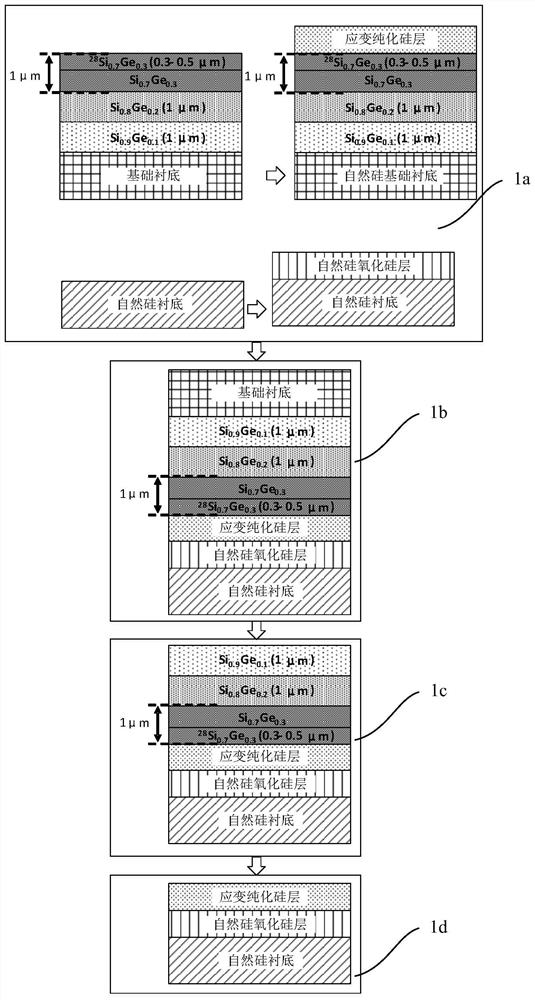
[0071] The strained purified silicon substrate in this embodiment includes a natural silicon substrate, a natural silicon oxide layer and a strained purified silicon layer stacked in sequence, see figure 1 , the specific formation method includes the following steps:

[0072] Step 1a: Provide a basic substrate, and epitaxially form four layers of silicon-germanium buffer layers on the basic substrate, which are respectively the first silicon-germanium buffer layer (Si 0.9 Ge 0.1 layer), the second silicon germanium buffer layer (Si 0.8 Ge 0.2 layer), the third silicon germanium buffer layer (Si 0.7 Ge 0.3 layer) and the fourth SiGe buffer layer ( 28 Si 0.7 Ge 0.3 layer), forming a strained purified silicon layer epitaxially on the fourth silicon germanium buffer layer to obtain a donor substrate;

[0073] Provide a natural silicon substrate, and form a layer of natural silicon oxide layer on the natural silicon substrate;

[0074] Step 1b: pressure bonding the donor s...

Embodiment 2

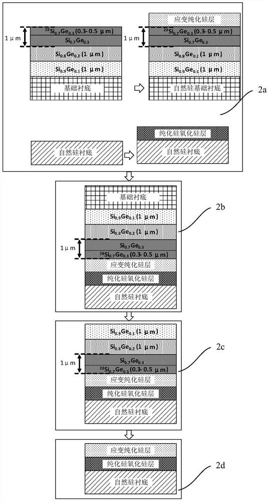
[0078] The strained purified silicon substrate in this embodiment includes a natural silicon substrate, a purified silicon oxide layer and a strained purified silicon layer stacked in sequence, see figure 2, the specific formation method includes the following steps:

[0079] Step 2a: Provide a basic substrate, and epitaxially form four layers of silicon-germanium buffer layers on the basic substrate, which are respectively the first silicon-germanium buffer layer (Si 0.9 Ge 0.1 layer), the second silicon germanium buffer layer (Si 0.8 Ge 0.2 layer), the third silicon germanium buffer layer (Si 0.7 Ge 0.3 layer) and the fourth SiGe buffer layer ( 28 Si 0.7 Ge 0.3 layer), forming a strained purified silicon layer epitaxially on the fourth silicon germanium buffer layer to obtain a donor substrate;

[0080] Provide a natural silicon substrate, and form a layer of pure silicon oxide layer on the natural silicon substrate;

[0081] Step 2b: pressure bonding the donor sub...

Embodiment 3

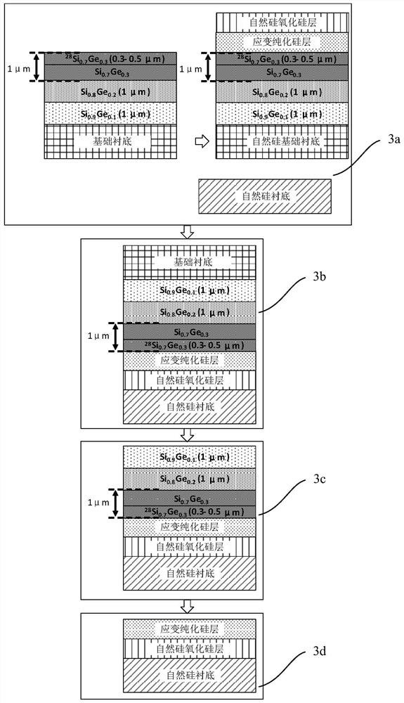
[0085] The strained purified silicon substrate in this embodiment has the same structure as the strained purified silicon substrate provided in Embodiment 1, including a natural silicon substrate, a natural silicon oxide layer and a strained purified silicon layer stacked in sequence, see image 3 , the specific formation method includes the following steps:

[0086] Step 3a: Provide a basic substrate, and epitaxially form four layers of silicon-germanium buffer layers on the basic substrate, which are respectively the first silicon-germanium buffer layer (Si 0.9 Ge 0.1 layer), the second silicon germanium buffer layer (Si 0.8 Ge 0.2 layer), the third silicon germanium buffer layer (Si 0.7 Ge 0.3 layer) and the fourth SiGe buffer layer ( 28 Si 0.7 Ge 0.3 layer), forming a strained purified silicon layer epitaxially on the fourth silicon germanium buffer layer, and forming a layer of natural silicon oxide silicon layer on the strained purified silicon layer to obtain a d...


PUM

PropertyMeasurementUnit
thicknessaaaaaaaaaa
thicknessaaaaaaaaaa
thicknessaaaaaaaaaa

Abstract

The invention discloses a strain purified silicon substrate for semiconductor quantum calculation and a forming method thereof, belongs to the technical field of semiconductors, and aims to solve theproblems that epitaxial purified silicon is greatly influenced by natural silicon isotope components of a substrate and the electron mobility of a purified silicon layer is low in the prior art. The strain purified silicon substrate comprises a natural silicon substrate, an insulating layer and a strain purification silicon layer, and tensile stress is introduced into the strain purification silicon layer. The forming method comprises the following steps: epitaxially forming a plurality of silicon-germanium buffer layers on a base substrate, gradually increasing the germanium doping concentration in the plurality of silicon-germanium buffer layers, and forming a strain purification silicon layer on the silicon-germanium buffer layers to obtain a donor substrate; providing a natural siliconsubstrate; forming an insulating layer on the donor substrate and/or the natural silicon substrate; and bonding the donor substrate with a natural silicon substrate, and removing the silicon-germanium buffer layer and the base substrate to obtain the strain purified silicon substrate. The strain purified silicon substrate and the forming method can be used for semiconductor quantum calculation.

Description

technical field [0001] The invention belongs to the technical field of semiconductors, in particular to a strained purified silicon substrate for semiconductor quantum computing and a forming method thereof. Background technique [0002] Integrated circuits continue to develop along Moore's Law, and the feature size has reached 5nm and below at this stage. In a small size, the "heat loss effect" of circuit heat dissipation makes the classical calculation have a calculation upper limit, and at the same time, a "size effect" will occur in a small size, so that the classical physical laws are no longer applicable. Quantum computing can use the superposition characteristics of quantum mechanics to realize the superposition of computing states. It not only has the 0 and 1 modes of classical computing, but also contains its superposition state. Due to this characteristic, it can realize strong parallelism of one-click processing of multiple inputs. Compared with traditional progr...

Claims


Application Information

Patent Timeline
Patent Type & Authority Applications(China)
IPC IPC(8): H01L21/02
CPCH01L21/02381H01L21/0245H01L21/02532H01L21/02488H01L21/0262B82Y10/00B82Y40/00
Inventor 王桂磊亨利·H·阿达姆松孔真真罗雪
Owner INST OF MICROELECTRONICS CHINESE ACAD OF SCI
Why Eureka
Try Eureka