Chip antenna with improved structure

A chip-type and antenna technology, applied in the direction of antenna, antenna grounding device, radiation element structure, etc., can solve the problem of different lengths of microstrip lines, and achieve the effect of high replaceability, simplified manufacturing process and components

Pending Publication Date: 2021-03-30
POWER WAVE ELECTRONICS
View PDF0 Cites 0 Cited by
  • Summary
  • Abstract
  • Description
  • Claims
  • Application Information

AI Technical Summary

Problems solved by technology

However, the length of the microstrip line may vary depending on the environment in which it is used, which will confuse users

Method used


Image

  • Chip antenna with improved structure
  • Chip antenna with improved structure
  • Chip antenna with improved structure

Examples


Embodiment Construction

[0043] The technical content and detailed description of the present invention are hereby described as follows in conjunction with the drawings:

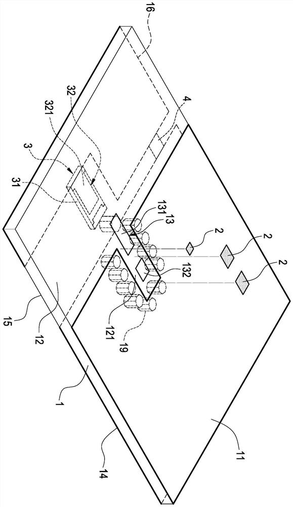
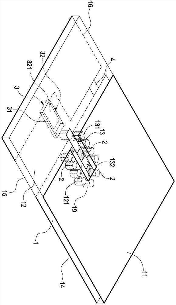
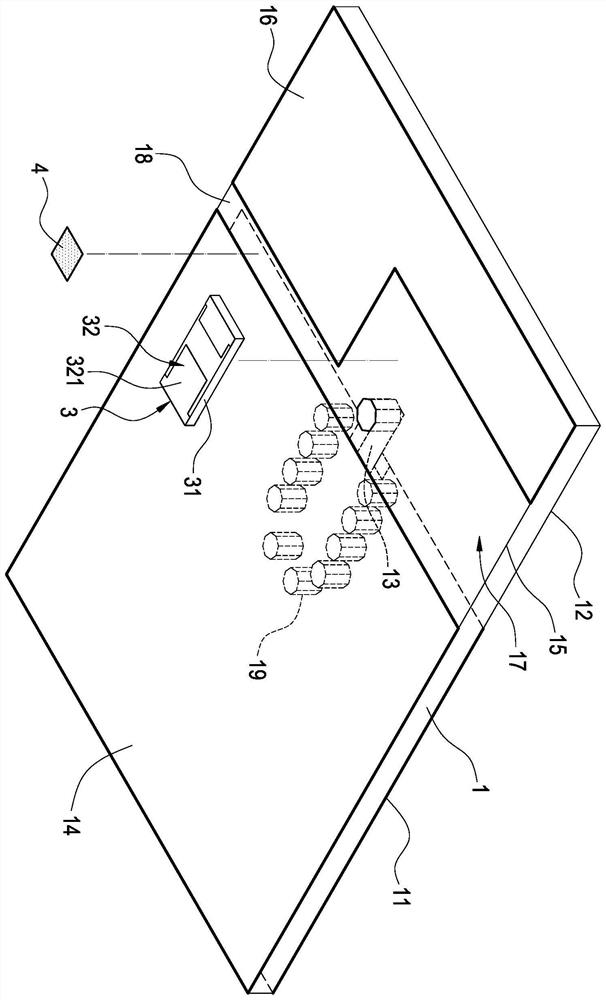
[0044] see figure 1 , 2 , is a schematic diagram of top component decomposition and top assembly of the chip antenna structure of the present invention. As shown in the figure: the top of the structurally improved chip antenna of the present invention includes: a substrate 1 and at least one matching element 2 .

[0045] The top of the substrate 1 has a concave first ground plane 11 , a convex first clearance area 12 and a signal feed-in unit 13 . The signal feed-in unit 13 is arranged on the first clearance area 12 and extends to the concave-convex junction 121 with the first ground plane 11. The signal feed-in unit 13 is composed of a plurality of metal wire segments 131, 132 .

[0046] The matching elements 2 are electrically connected between the metal wire segments 131 , 132 and the first ground plane 11 , and the impedance...


PUM


Abstract

The invention relates to an improved structure of a chip antenna. The improved structure comprises a substrate, at least one matching element, a radiation monomer and a frequency modulation element, wherein the substrate is provided with a first ground plane, a first clearance zone and a signal feed-in unit, and the other side of the substrate is provided with a second ground plane corresponding to the first ground plane, a second clearance zone corresponding to the first clearance zone, a third ground plane arranged in the second clearance zone, and a plurality of through substrates electrically connected with the first ground plane and the second ground plane. The matching element is electrically connected between the signal feed-in unit and the first ground plane. One end of the radiation unit is electrically connected with the signal feed-in unit through the via hole, and the other end of the radiation unit is electrically connected with the third ground plane. The frequency modulation element is electrically connected between the second ground plane and the third ground plane so as to adjust the frequency modulation element, i.e., the transceiving frequency of the antenna canbe adjusted.

Description

technical field [0001] The invention relates to an antenna, in particular to a chip antenna with an improved structure designed to extend metal sheets in the clearance area of ​​the chip antenna. Background technique [0002] With the popularity of the Internet, people are increasingly dependent on the Internet, and more and more mobile Internet devices have been developed, such as desktop computers, notebook computers, tablet computers, e-books (E-readers), smart phones, etc. When Internet access devices are popular in the market, it is also reported that people are concerned about the convenience of network information acquisition and network interpersonal interaction, and the second is the stability of communication system reception and transmission. [0003] The transmission or reception of these information mainly depends on the radio frequency (RF) wireless module (RF SiP Module) or RF system package components such as wireless local area network (Wi-Fi), 3G and global...

Claims


Application Information

Patent Timeline
IPC IPC(8): H01Q1/48H01Q1/50H01Q5/314H01Q1/38
CPCH01Q1/48H01Q1/50H01Q5/314H01Q1/38
Inventor 廖文照蔡昀展洪世勋杨士弘
Owner POWER WAVE ELECTRONICS
Why Eureka
Try Eureka