Light-emitting diode

A technology of light-emitting diodes and external electrodes, which is applied in the direction of electrical components, circuits, semiconductor devices, etc., can solve problems such as excessive cavity area, and achieve the effects of improving mechanical properties, increasing push-pull force levels, and improving photoelectric performance

Inactive Publication Date: 2021-04-16
SHENZHEN INST OF WIDE BANDGAP SEMICON
View PDF10 Cites 2 Cited by
  • Summary
  • Abstract
  • Description
  • Claims
  • Application Information

AI Technical Summary

Problems solved by technology

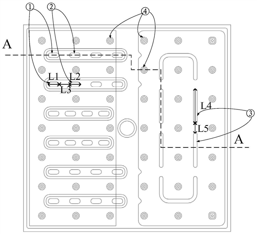
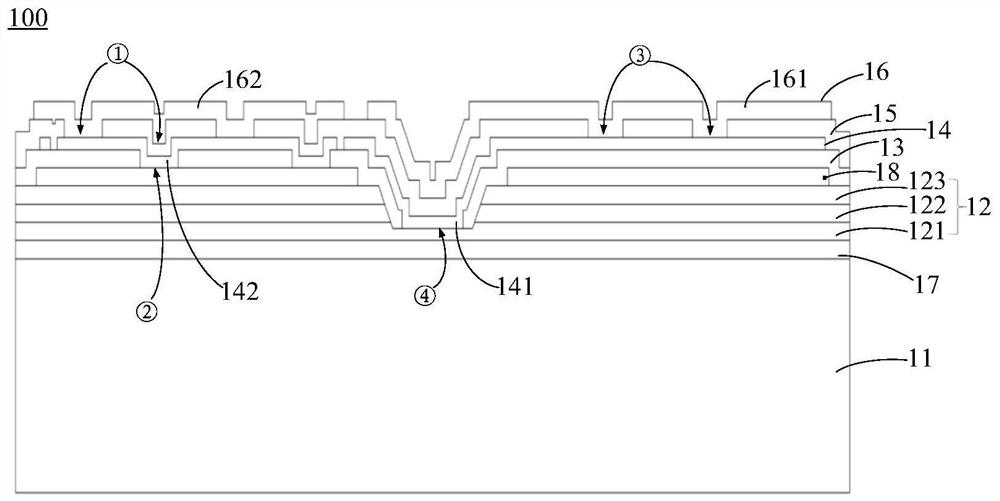
[0004] Based on this, the present application provides a light-emitting diode, which can solve the technical problems caused by the excessively large cavity area in the prior art,

Method used


Image

  • Light-emitting diode
  • Light-emitting diode
  • Light-emitting diode

Examples


Embodiment Construction

[0012] The following will clearly and completely describe the technical solutions in the embodiments of the application with reference to the drawings in the embodiments of the application. Apparently, the described embodiments are only some of the embodiments of the application, not all of them. Based on the embodiments in this application, all other embodiments obtained by persons of ordinary skill in the art without making creative efforts belong to the scope of protection of this application.

[0013] The terms "first", "second", "third", "fourth", etc. (if any) in the description and claims of this application and the above drawings are used to distinguish similar objects and not necessarily Describe a specific order or sequence. It is to be understood that the data so used are interchangeable under appropriate circumstances such that the embodiments of the application described herein can be practiced in sequences other than those illustrated or described herein. Furthe...


PUM


Abstract

The invention relates to the technical field of semiconductors, and particularly discloses a light-emitting diode comprising a substrate, an epitaxial layer, a first passivation layer, inner electrode layers, a second passivation layer and an outer electrode layer, wherein the second passivation layer is provided with fourth slots, and second outer electrode areas are electrically connected with a second inner electrode layer through the fourth slots; and larger than or equal to 2 fourth slots corresponding to each second outer electrode area are arranged, and the fourth slots are arranged at intervals. By means of the mode, the technical problem caused by the fact that a cavity area is too large in the prior art can be solved, the push-pull force level after the light-emitting diode and a packaging support are welded is improved, and the mechanical performance of a light-emitting diode packaging product is improved; and on the other hand, the uniformity of current diffusion and thermal diffusion of the light-emitting diode product can be improved, so that the photoelectric property and the application reliability of the light-emitting diode product are improved.

Description

technical field [0001] The present application relates to the technical field of semiconductors, in particular to a light emitting diode. Background technique [0002] In a conventional flip-chip light emitting diode, an N electrode and a P electrode are sequentially stacked on one side of the passivation layer, wherein a concave surface is formed on the surface of the P electrode. [0003] In the long-term research process, the inventors of the present application found that during the packaging process of the above-mentioned flip-chip light-emitting diodes, the solder material tends to produce cavities at the concave surface of the P electrode, resulting in a decrease in the push-pull force after the light-emitting diode and the package bracket are welded, affecting The reliability of the light-emitting diode packaging structure; in addition, the larger the cavity area, the smaller the current injection area, the worse the current injection uniformity, and the worse the he...

Claims


Application Information

Patent Timeline
IPC IPC(8): H01L33/38H01L33/44
Inventor 颜改革蒋振宇闫春辉
Owner SHENZHEN INST OF WIDE BANDGAP SEMICON
Why Eureka
Try Eureka