Preparation method of semiconductor device

A semiconductor and device technology, applied in the field of semiconductor device preparation, can solve problems such as low electro-optical conversion efficiency

Pending Publication Date: 2021-04-16
度亘激光技术(苏州)有限公司
View PDF3 Cites 0 Cited by
  • Summary
  • Abstract
  • Description
  • Claims
  • Application Information

AI Technical Summary

Problems solved by technology

[0004] The purpose of the present invention is to provide a method for preparing a semiconductor device to improve the low electro-optical conversion efficiency of the existing semiconductor device due to current diffusion.

Method used


Image

  • Preparation method of semiconductor device
  • Preparation method of semiconductor device
  • Preparation method of semiconductor device

Examples


Embodiment Construction

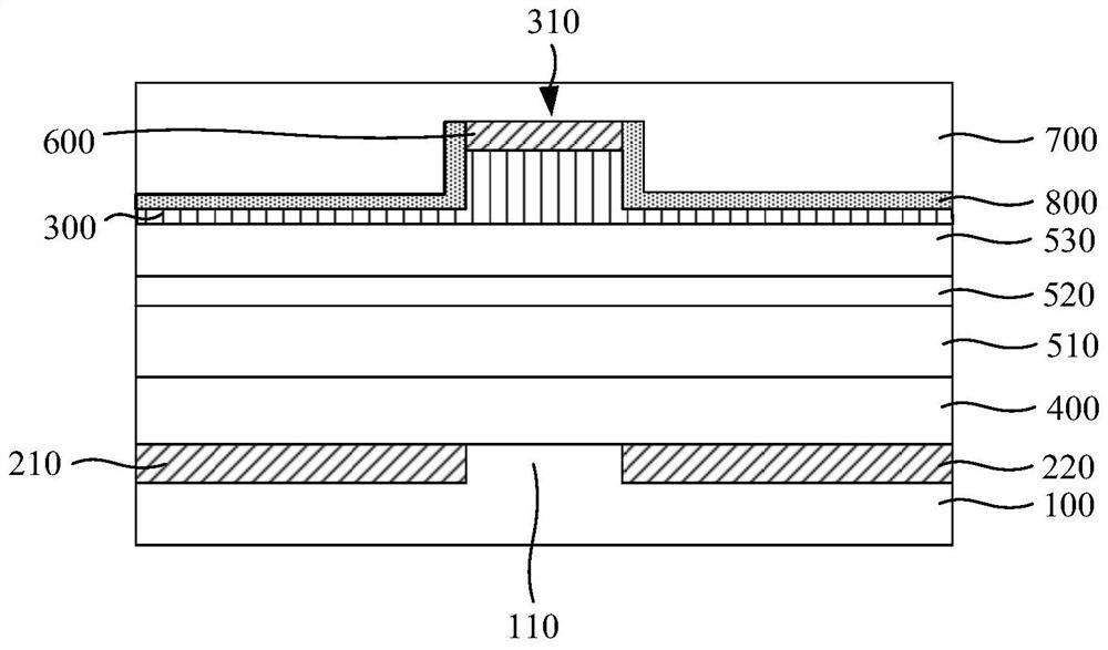
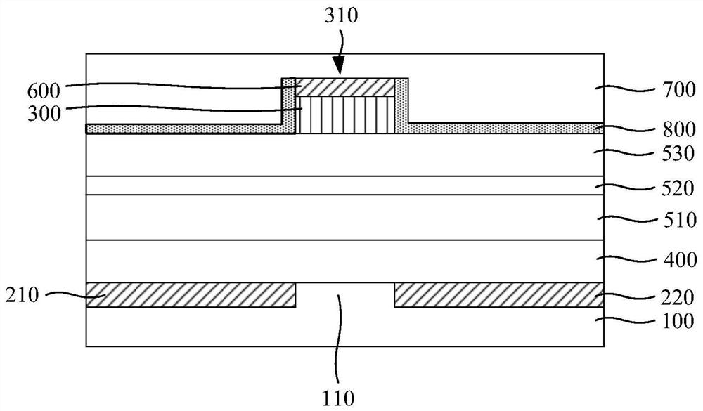
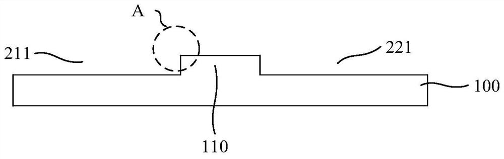
[0030] In order to make the purpose, technical solutions and advantages of the embodiments of the present invention clearer, the technical solutions in the embodiments of the present invention will be clearly and completely described below in conjunction with the drawings in the embodiments of the present invention. Obviously, the described embodiments It is a part of embodiments of the present invention, but not all embodiments. The components of the embodiments of the invention generally described and illustrated in the figures herein may be arranged and designed in a variety of different configurations.

[0031] Accordingly, the following detailed description of the embodiments of the invention provided in the accompanying drawings is not intended to limit the scope of the claimed invention, but merely represents selected embodiments of the invention. It should be noted that, in the case of no conflict, various features in the embodiments of the present invention can be com...


PUM


Abstract

The invention provides a preparation method of a semiconductor device, and relates to the technical field of semiconductors, a first current blocking region and a second current blocking region are formed on a substrate layer, and the part, between the first current blocking region and the second current blocking region, of the substrate layer is a channel region; a lower cladding layer, a waveguide layer and a ridge forming layer are formed on the substrate layer on which the first current blocking region, the channel region and the second current blocking region are formed; and the ridge forming layer is formed to form a ridge layer with a ridge structure. Part of the region of the ridge forming layer is etched through patterning, that is, the area of the orthographic projection, corresponding to the ridge strip structure, on the substrate layer is smaller than that before etching. The ridge strip structure is matched with the channel region to effectively control the path of the current, so that the current is more concentrated, and the electro-optical conversion efficiency of the device is further improved.

Description

technical field [0001] The invention relates to the technical field of semiconductors, in particular to a method for preparing a semiconductor device. Background technique [0002] Semiconductor devices are lasers that use semiconductor materials as working substances. They have many advantages such as small size, high efficiency, long life, and easy integration. Therefore, they are widely used in imaging, communication, machining and other fields. However, with the advancement of technology, there is also a higher demand for semiconductor devices. [0003] Existing semiconductor devices usually adopt a stacked semiconductor device epitaxial structure, but because it does not effectively control the conduction current, the electro-optical conversion efficiency is low. Contents of the invention [0004] The object of the present invention is to provide a method for manufacturing a semiconductor device to solve the problem of low electro-optical conversion efficiency caused...

Claims


Application Information

Patent Timeline
IPC IPC(8): H01S5/20H01S5/22
Inventor 杨国文唐松
Owner 度亘激光技术(苏州)有限公司
Why Eureka
Try Eureka