

Preparation method of OLED display panel and OLED display panel
A technology for display panels and substrates, which is applied in the manufacture of semiconductor/solid-state devices, electrical components, and electric solid-state devices, etc., can solve the problems of difficult control of precision and high difficulty in the manufacturing process of auxiliary electrodes, and achieves reduction of surface resistance and improvement of in-plane resistance. The effect of brightness uniformity
- Summary
- Abstract
- Description
- Claims
- Application Information
AI Technical Summary
Problems solved by technology
Method used
Image

Examples
Embodiment Construction
[0020] The following will clearly and completely describe the technical solutions in the embodiments of the present invention with reference to the drawings in the embodiments of the present invention. In the drawings, for clarity and ease of understanding and description, the size and thickness of the components shown in the drawings are not in scale.
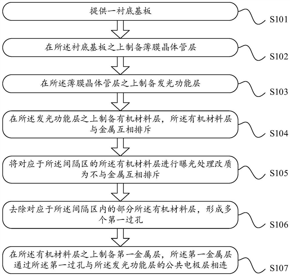
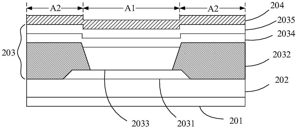
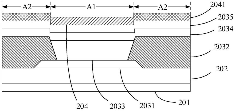
[0021] Such as figure 1 As shown, it is a flowchart of a method for preparing an OLED display panel provided by an embodiment of the present invention. The OLED display panel includes a plurality of pixels arranged in an array and a spacer between the plurality of pixels. The preparation method includes the following step:
[0022] S101. Provide a base substrate;
[0023] S102, preparing a thin film transistor layer on the base substrate;
[0024] S103, preparing a light-emitting functional layer on the thin film transistor layer;
[0025] S104. Prepare an organic material layer on the light-emitting functional layer, and ...
PUM
| Property | Measurement | Unit |
|---|---|---|
| Thickness | aaaaa | aaaaa |
Abstract
Description
Claims
Application Information