Dye sensitization photoelectric converter and process for fabricating the same

a photoelectric converter and dye sensitization technology, applied in the direction of sustainable manufacturing/processing, final product manufacturing, electrochemical generators, etc., can solve the problems of low photoelectric transfer efficiency of amorphous silicon solar cells, needing an evacuation process for manufacture, and inability to absorb sensitizing dye particles, etc., to suppress association of sensitizing dye particles, enhance photoelectric transfer efficiency, and increase the quantity of sensitizing dye absorbed

Inactive Publication Date: 2006-04-20
SONY CORP
View PDF33 Cites 30 Cited by
  • Summary
  • Abstract
  • Description
  • Claims
  • Application Information

AI Technical Summary

Benefits of technology

[0015] The Inventors of the present invention made researches to solve the aforementioned problems involved in the existing techniques, and found that the use of titania nanotubes as the semiconductor layer is most effective to enable sensitizing dyes having no acidic substituents. Thus, the Inventors have reached the present invention.
[0027] The transparent conductive substrate may be made by forming a transparent conductive film on a conductive or non-conductive transparent support substrate, or may be an electrically conductive transparent substrate in its entirety. There is no particular limitation to the material of the conductive substrate, and various kinds of transparent support materials are usable. The conductive substrate preferably has high blocking capability against intruding moisture and gas from outside the photoelectric transfer element, high resistance to the solvent and high weather resistance. Examples of such substrates are transparent inorganic substrates of quartz, glass, or the like, transparent plastic substrates of polyethylene terephthalate, polyethylene naphthalate, polycarbonate, polystyrene, polyethylene, polypropylene, polyphenylene sulfide, polyvinylidene fluoride, tetraacetyl cellulose, phenoxy bromide, kinds of aramid, kinds of polyimide, kinds of polystyrene, kinds of polyarylate, kinds of polysulfone, kinds of polyolefin, and so forth. However, materials of the substrate are not limited to these examples. Taking easier workability and lighter weight into account, a transparent plastic substrate is preferably used as the conductive substrate. There is no particular limitation to the thickness of the conductive substrate. The thickness may be determined freely depending upon the light transmittance, blocking capability between the inside and the outside of the photoelectric transfer element, and other factors.
[0028] It is desirable that the transparent conductive substrate has surface resistance as low as possible. More specifically, the surface resistance of the transparent conductive substrate is preferably 500 Ω / □ or less, and more preferably 100 Ω / □ or less. In case the conductive substrate is made by forming a transparent conductive film on a transparent support substrate, known materials can be used. Examples of such materials are indium-tin complex oxide (ITO) fluorine-doped ITO (FTO) and SnO2. Usable materials are not limited to those examples, and two or more of them can be used in combination as well. For the purpose of reducing the surface resistance of the transparent conductive substrate and thereby enhancing the collecting efficiency, a pattern of metal wiring of high conductivity can be made on the transparent conductive substrate.
[0031] Specific surface area of titania nanotubes is 270 m2 / g, which is exponentially larger than the specific surface area (50 m2 / g) of anatase crystals of porous titania generally used in dye-sensitized solar cells. Therefore, it is possible to increase the quantity of the sensitizing dye absorbed and greatly enhance the photoelectric transfer efficiency.
[0032] Since there is no need of introducing acidic substituents into the sensitizing dye, it is possible to suppress association of sensitizing dye particles, thereby alleviate the phenomenon of optical quenching of photo-excited electrons, and efficiently inject excited electrons into the titania nanotubes. This advantage also contributes to enhancing the photoelectric transfer efficiency.
[0033] In addition, no need of introducing acidic substituents into the sensitizing dye simplifies the manufacturing process of the sensitizing dye and thereby contributes to great reduction of the manufacturing cost. At the same time, since the need of introduction of acidic substituents is removed, it is easy to use new sensitizing dyes having been unknown heretofore, and the liberty of choice of sensitizing dyes is broadened.

Problems solved by technology

However, since crystalline silicon solar cells need much energy and time for crystal growth, they are disadvantageous in terms of the cost because of the low productivity.
However, photoelectric transfer efficiency of amorphous silicon solar cells is lower than that of crystalline silicon solar cells.
Furthermore, although amorphous silicon solar cells are higher in productivity than crystalline silicon solar cells, they need an evacuation process for the manufacture, and still consume high energy.
In addition, these solar cells involve the problem of environmental pollution because toxic materials such as gallium, arsenic and silane gas are used for the manufacture.
However, many of them have poor photoelectric transfer coefficient as low as 1% and have not be turned into practical use.
However, since the sensitizing dye used in the above-introduced technique is used in the form absorbed by porous titania, it must have acidic substituents such as carboxylic acid, and this has restricted sensitizing dyes usable.
Furthermore, because of the introduction of acidic substituents to the sensitizing dye, the manufacturing cost of such sensitizing dye was inevitably high, and inevitably increased the manufacturing cost of dye-sensitized solar cells.
Moreover, introduction of acidic substituents to sensitizing dye increases the liability to association of sensitizing dyes with each other via the acidic substituents, and brings about the phenomenon of optical quenching of photo-excited electrons, thereby decreasing the injection efficiency of excitation electrons into semiconductors.
Therefore, it has been difficult to obtain sufficient effect of enhancing photoelectric transfer efficiency by introduction of the sensitizing dye.
As such, existing dye-sensitized solar cells involve the problem that employable sensitizing dyes are limitative because of their acidic substituents as well as the problem that their practical use are difficult because of high manufacturing costs caused by sensitizing dyes requiring a complicated manufacturing process and limits of enhancement in photoelectric transfer efficiency.

Method used


Image

  • Dye sensitization photoelectric converter and process for fabricating the same
  • Dye sensitization photoelectric converter and process for fabricating the same
  • Dye sensitization photoelectric converter and process for fabricating the same

Examples


embodiment

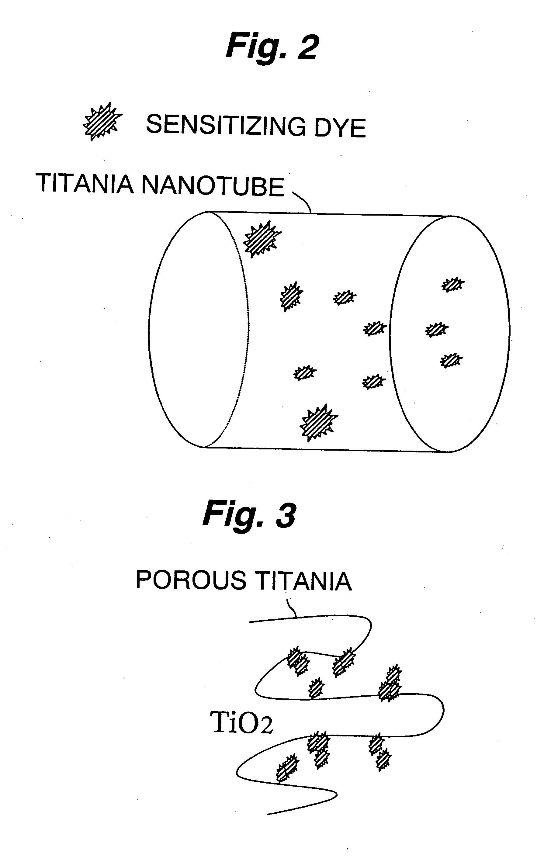
[0060] Referring to Japanese Patent Laid-open Publication JP-H10-152323, titania nanotubes were fabricated as explained below. Commercially available crystal titania (mean grain size: 20 nm; specific surface area: 50 m2 / g) was immersed into 40 wt % sodium hydroxide solution and left to react in a hermetic container for 20 hours at 110° C.

[0061] Next referring to H. Arakawa, “Latest Techniques of Dye-sensitized Solar Cells” (C.M.C.) p. 45-47 (2001), paste of titania nanotubes was prepared as follows. Titania nanotubes were dispersed in an ethanol solution to contain 11 wt % of titania nanotubes. Then, the solution was added with PEO having the molecular mass of 500 thousands, and mixed homogenously in a planet ball mill to obtain a viscosity-enhanced paste of titania nanotubes.

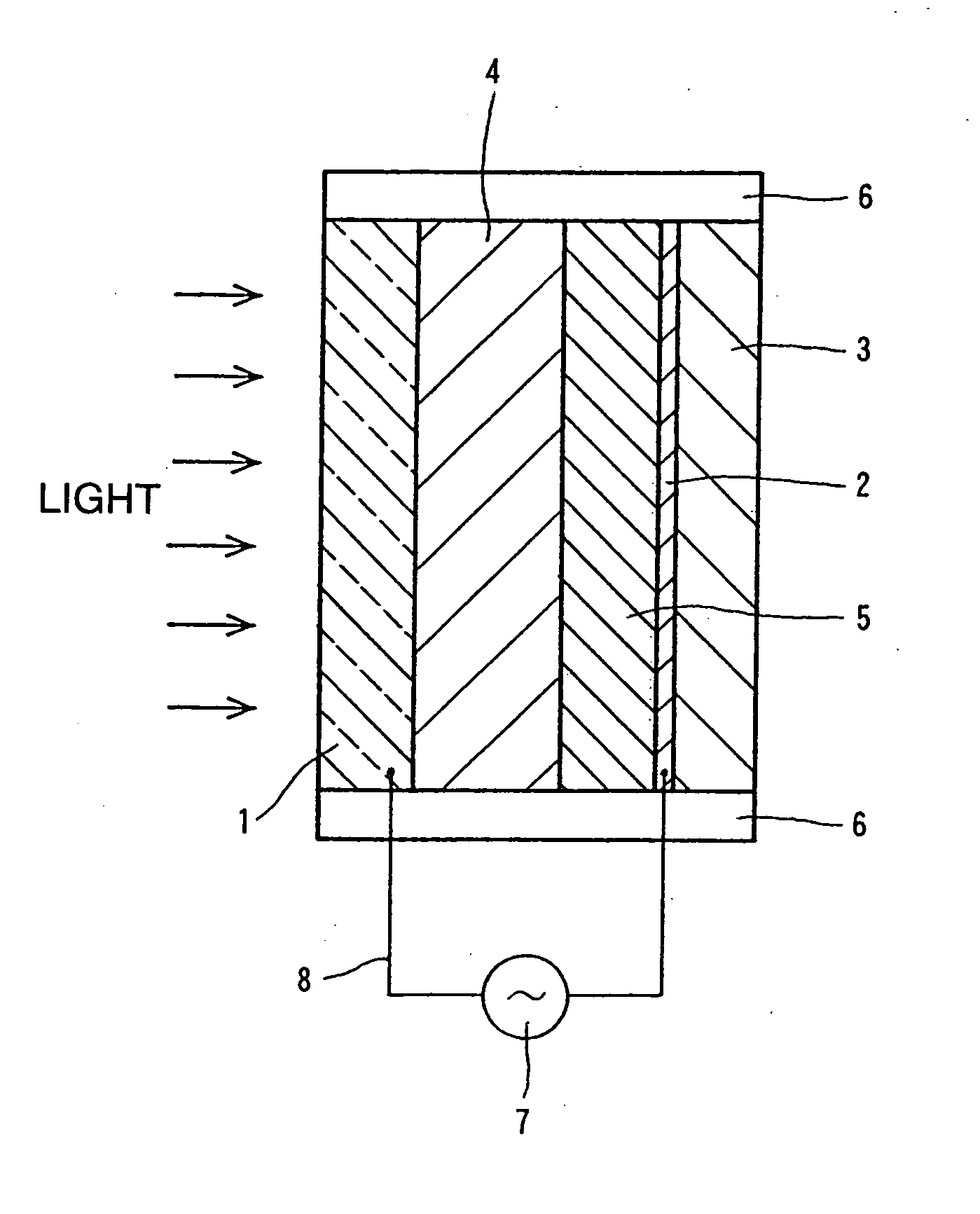
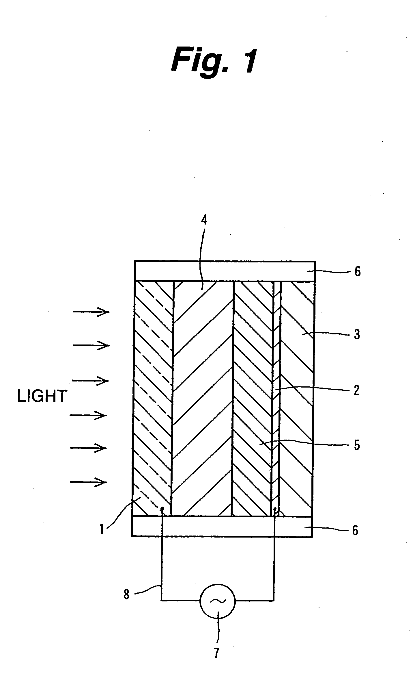
[0062] The paste of titania nanotubes obtained was coated on a fluorine-doped conductive glass substrate (sheet resistance: 30 Ω / □) over the area of 1 cm×1 cm by screen printing, then maintained at 450° C. fo...


PUM

PropertyMeasurementUnit
diameteraaaaaaaaaa
diametersaaaaaaaaaa
specific surface areaaaaaaaaaaa

Abstract

In a dye-sensitized photoelectric transfer device having a semiconductor layer and an electrolyte layer between a transparent conductive substrate and a counter conductive substrate, the semiconductor layer is composed of titania nanotubes, and a sensitizing dye is retained by the titania nanotubes. The titania nanotubes preferably have an anatase-type crystalline form. The dye-sensitized photoelectric transfer device is used as a dye-sensitized solar cell.

Description

TECHNICAL FIELD [0001] The present invention relates to a dye-sensitized photoelectric transfer device and a manufacturing method thereof, especially suitable for application to dye-sensitized solar cells. BACKGROUND ART [0002] Various solar cells have been developed as energy source using sunlight in place of fossil oil. The most popular solar cells use silicon, and a number of such solar cells are commercially available. They are roughly classified to crystalline silicon solar cells using single crystal silicon or polycrystal silicon and amorphous silicon solar cells. [0003] Solar cells have often used single crystal silicon or polycrystal silicon, i.e. crystalline silicon. [0004] In crystalline silicon solar cells, photoelectric transfer efficiency, which exhibits the performance of converting light (sun) energy to electrical energy, is higher than that of amorphous silicon solar cells. However, since crystalline silicon solar cells need much energy and time for crystal growth, t...

Claims


Application Information

Patent Timeline
Patent Type & Authority Applications(United States)
IPC IPC(8): H01L21/44H01G9/20H01L31/04H01L31/042H01M14/00
CPCB82Y10/00H01G9/2031Y02E10/542H01M14/005H01G9/2063Y02P70/50H01L31/04H01M14/00
Inventor TOKITA, YUICHISUZUKI, YUSUKEMOROOKA, MASAHIROISHIBASHI, KENICHINODA, KAZUHIRO
Owner SONY CORP
Why Eureka
Try Eureka