Optical Article and Method for Producing the Same

a technology of optical articles and optical elements, applied in the field of optical articles, can solve the problems of low resistance of compounds and production costs, and achieve the effects of reducing the resistance of the surface of the first layer, low cost, and reducing the resistance of the first layer (surface region)

Inactive Publication Date: 2010-09-09
HOYA LENS MFG PHILIPPINES
View PDF63 Cites 30 Cited by
  • Summary
  • Abstract
  • Description
  • Claims
  • Application Information

AI Technical Summary

Benefits of technology

[0007]One aspect of the invention provides a method for producing an optical article having a filter layer formed directly or with another layer in between on an optical substrate, the filter layer transmitting light in a predetermined wavelength band and blocking light with a wavelength longer and / or shorter than the predetermined wavelength band. The production method comprises forming a first layer to be included in the filter layer and adding at least one of carbon, silicon, and germanium to the surface of the first layer, thereby reducing the resistance of the surface of the first layer. Carbon, silicon, and germanium have been used as materials for household products, materials for semiconductor substrates, etc., and are available at relatively low cost. Further, the addition of these materials (composition) to the layer surface is possible by relatively simple methods, such as deposition (ion-assisted deposition), sputtering, and the like. Further, as a result of the addition to the layer surface, the layer surface is modified by the carbon, silicon, or germanium, whereby the resistance of the layer surface (surface region) can be reduced. In addition, carbon, silicon, and germanium form a compound with a transition metal, and in most cases, such compounds have low resistance. Therefore, as a result of the addition of carbon, silicon, and germanium to the surface of the first layer, accompanied by the formation of a compound in the surface region of the first layer, the resistance of the surface region can be reduced.

Problems solved by technology

However, in some uses, an ITO film may give concerns about durability, especially durability against sweat and like acids or alkali and like chemicals.
Lamination of thin films of noble metals has also been proposed, but it may be problematic in terms of production cost.
In addition, carbon, silicon, and germanium form a compound with a transition metal, and in most cases, such compounds have low resistance.

Method used


Image

  • Optical Article and Method for Producing the Same
  • Optical Article and Method for Producing the Same
  • Optical Article and Method for Producing the Same

Examples


example 1

Sample S1

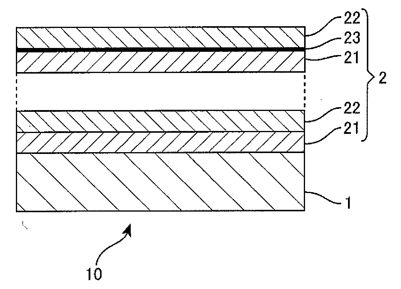
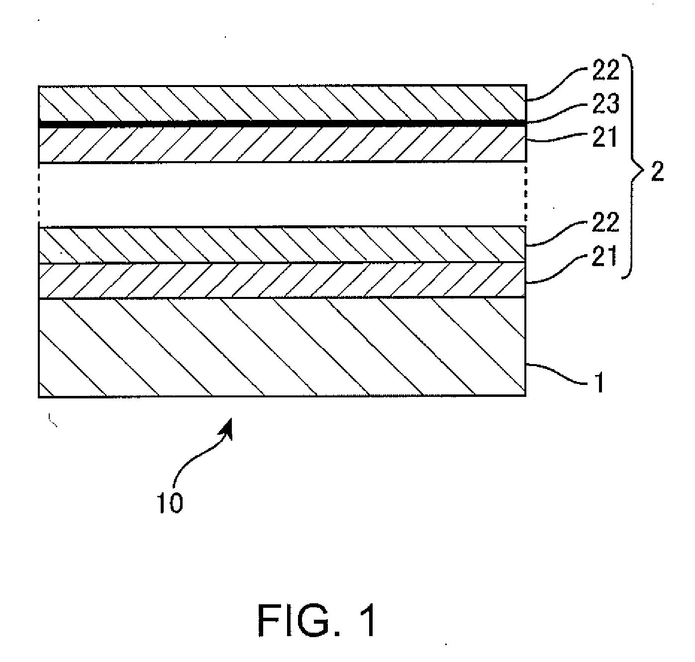
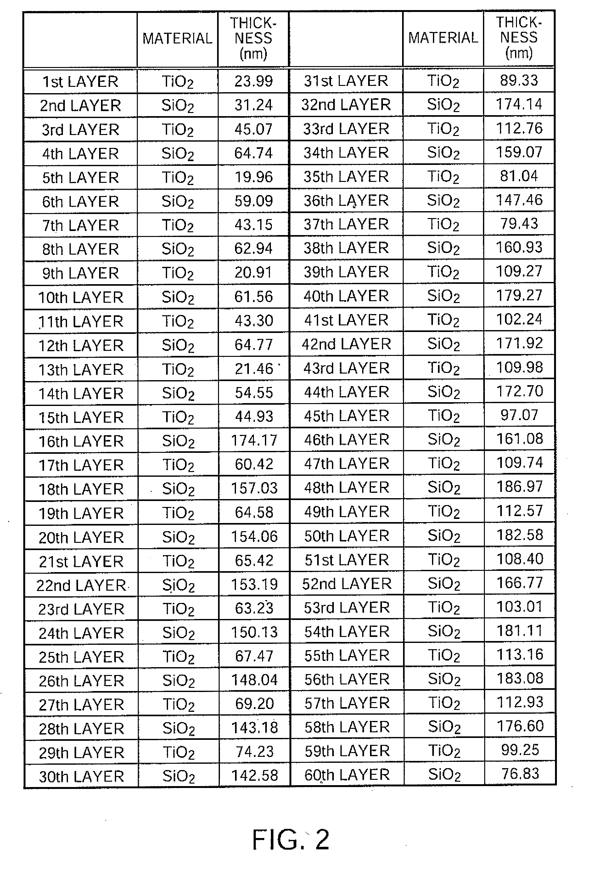
[0040]The substrate 1 herein is a glass substrate for transmitting light. In Example 1, a clear glass (B270) with a refractive index of 1.53 was used. Further, a filter layer 2 of an inorganic thin film was formed on the substrate 1 by ordinary ion-assisted, electron beam deposition (so-called IAD method), giving an optical multilayer filter 10. In Example 1, high-refractive-index layers 21 in the filter layer 2 are titanium oxide (TiO2) layers, and low-refractive-index layers 22 are silicon dioxide (SiO2) layers. Specifically, the substrate 1 was placed in a vacuum deposition chamber (not illustrated). A crucible fined with a deposition material was then placed at the bottom of the vacuum deposition chamber, and evaporated by an electron beam. Simultaneously, ionized oxygen was accelerated and irradiated using an ion gun (Ar was added in the case of TiO2 film formation), thereby alternately forming films to the thickness shown in FIG. 2.

[0041]The conditions for forming TiO...

example 2

Sample S2

[0056]In the same manner as in Example 1, an optical multilayer filter 10 including a filter layer 2 with the same structure as in Example 1 was produced. However, the conditions for reducing resistance are as follows.

Conditions for Reducing Resistance (Sample S2)

[0057]Subject layer: TiO2

Added composition: Silicon

Treatment time: 10 seconds

Ion irradiation conditions

[0058]Accelerating voltage: 500 V

[0059]Accelerating current: 150 mA

[0060]Ar flow rate: 20 sccm

Treatment temperature: 150° C.

[0061]After the filter layer 2 was formed, oxygen plasma treatment was performed. Subsequently, in a deposition apparatus, a high-molecular-weight, fluorine-containing organosilicon compound “KY-130” (trade name, manufactured by Shin-Etsu Chemical) was deposited to form an antifouling layer on the filter layer 2. Specifically, a pellet material containing the fluorine-containing organosilicon compound, as the deposition source, was heated at about 500° C. to form the antifouling layer. The d...

example 3

Sample S3

[0062]In the same manner as in Example 1, an optical multilayer filter 10 including a filter layer 2 with the same structure as in Example 1 was produced. However, the conditions for reducing resistance are as follows.

Conditions for Reducing Resistance (Sample S3)

[0063]Subject layer: TiO2

Added composition: Germanium

Treatment time: 10 seconds

Ion irradiation conditions

[0064]Accelerating voltage: 800 V

[0065]Accelerating current: 150 mA

[0066]Ar flow rate: 20 sccm

Treatment temperature: 150° C.


PUM


Abstract

A method for producing an optical article having a filter layer formed directly or with another layer in between on an optical substrate, the filter layer transmitting light in a predetermined wavelength band and blocking light with a wavelength longer and/or shorter than the predetermined wavelength band, includes: forming a first layer to be included in the filter layer, and adding at least one of carbon, silicon, and germanium to the surface of the first layer, thereby reducing the resistance of the surface of the first layer.

Description

BACKGROUND[0001]1. Technical Field[0002]The present invention relates to an optical article with filtering function and a method for producing the same.[0003]2. Related Art[0004]JP-A-2007-298951 (Patent Document 1) discloses an optical multilayer filter capable of maintaining antistatic effect over a long period of time without degradation of optical properties and a method for producing an optical multilayer filter for easily producing such a filter. Further, for the production of an electronic device having incorporated therein such an optical multilayer filter, Patent Document 1 also discloses that, with respect to a multilayer inorganic thin film formed on the substrate of the optical multilayer filter, the density of a silicon oxide layer that forms the outermost layer of the inorganic thin film is 1.9 to 2.2 g / cm3.[0005]According to Patent Document 1, the degree of vacuum during deposition is changed to reduce the density of the SiO2 film forming the outermost layer, thereby r...

Claims


Application Information

Patent Timeline
Patent Type & Authority Applications(United States)
IPC IPC(8): G02B5/20B05D5/06
CPCG02B5/208
Inventor NISHIMOTO, KEIJINOGUCHI, TAKASHISEKI, HIROYUKI
Owner HOYA LENS MFG PHILIPPINES
Why Eureka
Try Eureka