HDM-to-eDP interface conversion device and interface conversion method based on an FPGA

An interface conversion and hardware interface technology, which is applied in the field of interface conversion devices from HDM to eDP, and can solve the problems of slow display speed of 4K video images and difficult performance of image data transmission functions.

Active Publication Date: 2021-04-27
CHANGSHA XIANGJI HAIDUN TECH CO LTD
View PDF10 Cites 0 Cited by
  • Summary
  • Abstract
  • Description
  • Claims
  • Application Information

AI Technical Summary

Problems solved by technology

[0002] At present, the solutions commonly used by major LCD display manufacturers to light up 4K eDP interface LCD panels are based on Taiwan MSTAR or Realtek and Chinese mainland HiSilicon image processing chips, etc. It is designed by eDP processing chip, but it is very difficult to add new image data transmission function or change a certain performance by adopting this solution, such as adding a sub-screen eDP display or VGA ring-out display on the basis of the main screen eDP display Images with different resolutions cannot be implemented with the above scheme
And the display speed of the liquid crystal panel of this technical scheme is slow to 4K video image

Method used


Image

  • HDM-to-eDP interface conversion device and interface conversion method based on an FPGA
  • HDM-to-eDP interface conversion device and interface conversion method based on an FPGA
  • HDM-to-eDP interface conversion device and interface conversion method based on an FPGA

Examples


Embodiment Construction

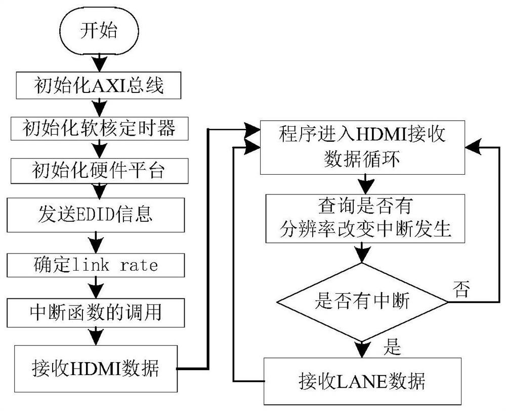
[0039] The following is a detailed description of the embodiments of the present invention. This embodiment is carried out based on the technical solution of the present invention, and provides detailed implementation methods and specific operation processes to further explain the technical solution of the present invention.

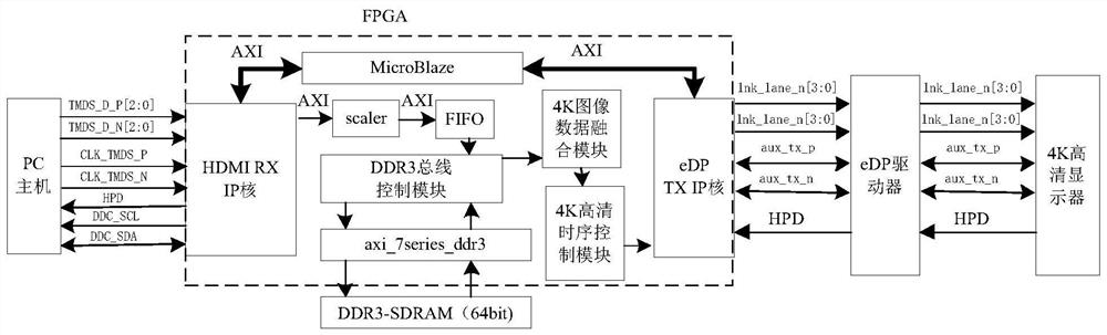
[0040] The present invention provides a FPGA-based HDM-to-eDP interface conversion device, refer to figure 1 As shown, it includes FPGA module and DDR3 SDRAM; the FPGA module includes HDMI RX module, MicroBlaze soft core module, scaler scaling module, FIFO module, DDR3 bus control module, DDR3 IP core module, 4K image data fusion module, 4K HD Timing control module and eDP TX module.

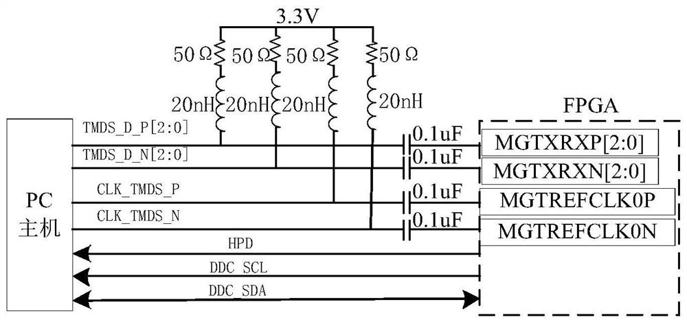
[0041] The HDMI RX module is connected to the PC host through the HDMI RX hardware interface, controlled by the MicroBlaze soft-core module, and receives video image data from the PC host; in this embodiment, the PC host needs to be installed with an output resolution of 3...


PUM


Abstract

The invention discloses an HDM-to-eDP interface conversion device and interface conversion method based on an FPGA. An FPGA module in the device comprises an HDMI RX module, a MicroBlaze soft core module, a scaler scaling module, an FIFO module, a DDR3 bus control module, a DDR3 IP core module, a 4K image data fusion module, a 4K high-definition time sequence control module and an eDP TX module. The HDMI RX module receives a video image from the PC host; the HDMI RX module converts the HDMI video image into an RGB format; the scaler scaling module amplifies the resolution of the video image in the RGB format to 4K, and the resolution is stored by the FIFO module; when the number of the stored data of the FIFO module reaches a preset pixel point number, the currently stored pixel point is stored into the DDR3 SDRAM; the 4K image data fusion module reads data from the DDR3 SDRAM for preprocessing, then the data is converted into an eDP signal by the 4K high-definition sequential control module, and the eDP signal is sent to the high-definition display by the eDP TX hardware interface. According to the invention, the display speed of the 4K high-definition liquid crystal display is high.

Description

technical field [0001] The invention relates to the field of 4K high-definition liquid crystal display systems, in particular to an FPGA-based HDM-to-eDP interface conversion device and an interface conversion method. Background technique [0002] At present, the solution commonly used by major LCD manufacturers to light up 4K eDP interface LCD panels is designed based on eDP processing chips such as MSTAR or Realtek in Taiwan, China, and Hisilicon image processing chips in mainland China. If this solution needs to add new It is particularly difficult to transfer image data or change a certain performance. For example, adding a sub-screen eDP display on the basis of the main screen eDP display or VGA ring output to display images with different resolutions cannot be realized by the above solutions. Moreover, the liquid crystal panel of this technical solution has a slow display speed for 4K video images. Contents of the invention [0003] The technical problem to be solve...

Claims


Application Information

Patent Timeline
Patent Type & Authority Applications(China)
IPC IPC(8): H04N5/268H04N5/765H04N7/015
CPCH04N5/765H04N7/015H04N5/268Y02D10/00
Inventor 赵小珍谢绪煜刘学满李文斌
Owner CHANGSHA XIANGJI HAIDUN TECH CO LTD
Why Eureka
Try Eureka