Eureka AIR delivers breakthrough ideas for toughest innovation challenges, trusted by R&D personnel around the world.

Semiconductor package and manufacturing method thereof

A manufacturing method and semiconductor technology, applied in semiconductor/solid-state device manufacturing, semiconductor devices, semiconductor/solid-state device components, etc., can solve problems such as tin bridge short circuit

Pending Publication Date: 2021-04-30
ADVANCED SEMICON ENG INC
View PDF0 Cites 0 Cited by
  • Summary
  • Abstract
  • Description
  • Claims
  • Application Information

AI Technical Summary

Problems solved by technology

However, when the line width is reduced, it may be due to the unavoidable drum-side effect during soldering, which may lead to solder bridges and cause short circuits. 20 µm) are often overlooked in structures

Method used


Image

  • Semiconductor package and manufacturing method thereof
  • Semiconductor package and manufacturing method thereof
  • Semiconductor package and manufacturing method thereof

Examples


Embodiment Construction

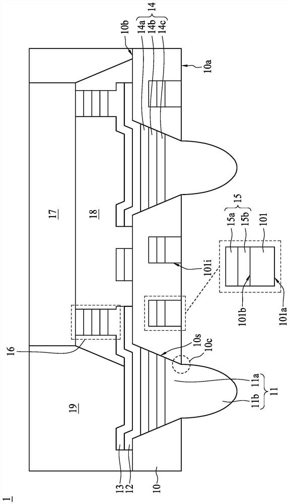
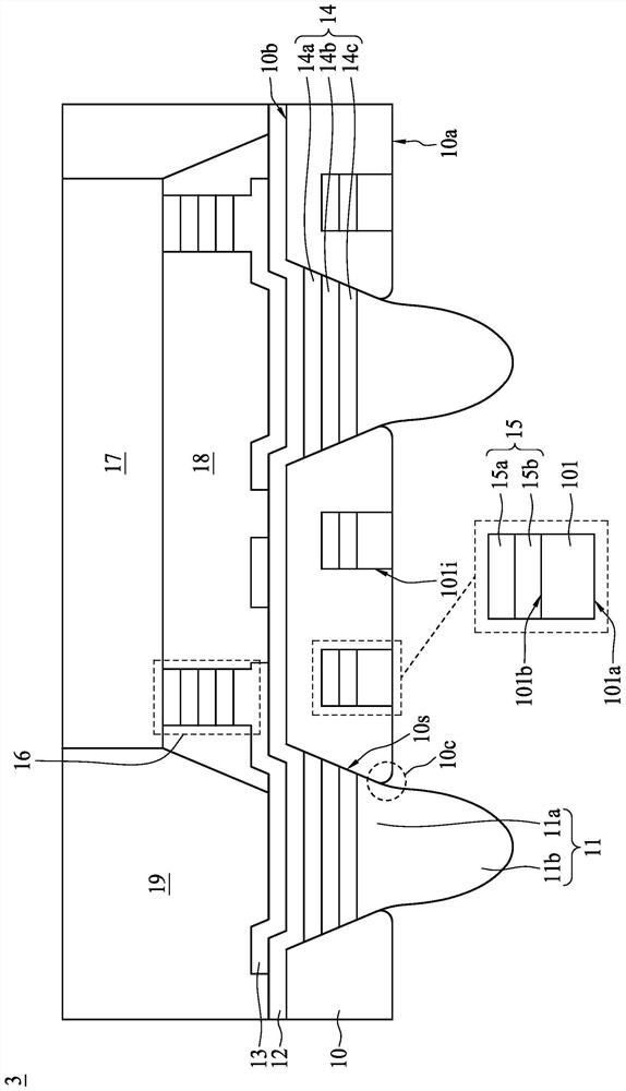
[0013] According to some embodiments, the present invention provides a semiconductor package combining a fine-pitch interconnect structure and a coarse-pitch interconnect structure, the fine-pitch interconnect structure being embedded in a single dielectric layer and separated from the conductive contacts by an insulating layer. Therefore, tin bridge generation can be avoided. In addition, only a single dielectric layer can be used to increase the circuit density per unit volume without using a multi-layer structure, which will reduce the thickness and manufacturing cost of semiconductor packaging devices, and can avoid warpage due to increased thickness. Phenomenon.

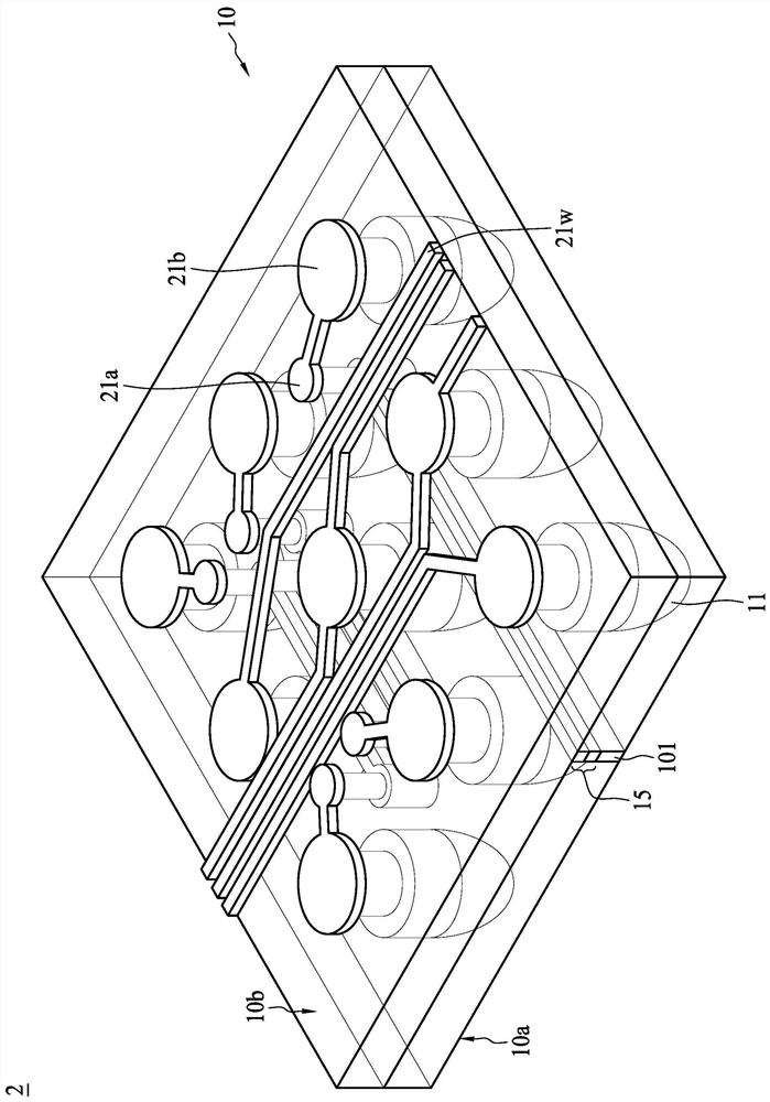
[0014] refer to figure 1 , figure 1 Shown is a cross-sectional view of a semiconductor package 1 according to some embodiments of the present disclosure. The semiconductor package 1 includes a substrate 10, a conductive contact 11, a seed layer 12, a metal layer 13, a conductive pillar 14, a metal layer 15, a...


PUM


Abstract

Embodiments of the present disclosure relate to a semiconductor package. The semiconductor package includes a substrate, a conductive pillar, and a metal layer. The substrate has a first surface, a second surface opposite to the first surface, and an opening extending from the first surface to the second surface. The opening is provided with a side wall, and the conduction column is arranged in the opening. The metal layer is arranged in the substrate. The metal layer and the conductive pillar are substantially located at the same horizontal height. Another embodiment of the present disclosure relates to a manufacturing method of the semiconductor package.

Description

technical field [0001] The present invention relates to a semiconductor package and a manufacturing method thereof, and more particularly, to a semiconductor package having a metal layer and an insulating layer encapsulating the metal layer. Background technique [0002] As the demand for high line density per unit volume increases, reducing the line width / space (L / S) is a method for increasing the line density per unit volume. However, when the line width is reduced, it may be due to the unavoidable drum-side effect during soldering, which may lead to solder bridges and cause short circuits. 20 μm) structures are often overlooked. Contents of the invention [0003] Embodiments of the disclosure relate to a semiconductor package. The semiconductor package includes a substrate, a conductive pillar, and a metal layer. The substrate has a first surface, a second surface opposite to the first surface, and an opening extending from the first surface to the second surface. T...

Claims


Application Information

Patent Timeline
IPC IPC(8): H01L23/498H01L21/48
CPCH01L23/49838H01L23/49822H01L21/4857H01L2924/181H01L2224/73204H01L2924/18161H01L2924/00012
Inventor 呂文隆
Owner ADVANCED SEMICON ENG INC
Why Eureka
Eureka Blog
Learn More