PNP-type high-voltage ESD device based on BCD process, and LDMOS
An ESD device, high-voltage technology, applied in the field of LDMOS, PNP type high-voltage ESD devices, can solve the problems of high on-resistance, high secondary breakdown voltage, low secondary breakdown current, etc., to improve performance and reduce volume Effect
- Summary
- Abstract
- Description
- Claims
- Application Information
AI Technical Summary
Problems solved by technology
Method used
Image

Examples
Embodiment 1
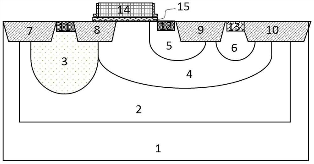
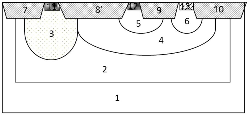
[0035] Such as figure 1 As shown, this embodiment discloses a PNP-type high-voltage ESD device based on BCD technology, including a P substrate 1, a high-voltage N well 2, a P-type drift region 3, an N-type drift region 4, a first N well 5, a first Two N-wells 6 , N-type base 13 , P-type collector 11 , P-type emitter 12 , polysilicon gate 14 , gate oxide layer 15 , first STI8 , second STI7 , third STI9 and fourth STI10 . Among them, the PNP high-voltage ESD device is a PNP transistor; the working voltage range is 40-65V; the node range of the BCD process is 65-180nm.
[0036] Wherein, the first STI 8 is located between the P-type collector 11 and the P-type emitter 12 . The polysilicon gate 14 is located in the upper region of the two ends adjacent to the first STI 8 and the P-type emitter 12 . The gate oxide layer 15 is located between the polysilicon gate 14 and the second STI 8 and the P-type emitter 12 . The high-voltage N well 2 is located in the P substrate 1; the P-t...
Embodiment 2
[0042] This embodiment discloses an LDMOS, which is a high-voltage LDMOS, including the BCD-based PNP high-voltage ESD device disclosed in Embodiment 1. Among them, the PNP high-voltage ESD device based on the BCD process is used to realize the ESD protection of the high-voltage LDMOS. When the peak voltage caused by the instantaneous current exceeds its 40-65V working voltage but does not reach the secondary breakdown voltage, the LDMOS guides the current through the PNP high-voltage ESD device to achieve ESD protection. In this embodiment, by adjusting the structure of the PNP-type high-voltage ESD device, a higher secondary breakdown current It2, a lower on-resistance Ron and a lower The secondary breakdown voltage Vt2. The volume of the device can be reduced, and the performance of the device can be greatly improved.
PUM
 Abstract
Description
Claims
Application Information